Method of fabricating a MOSFET device with metal containing gate structures

a gate structure and metal containing technology, applied in the direction of semiconductor devices, electrical equipment, transistors, etc., can solve the problems of incompatibility of metal gate structures with wet etch procedures used with self-alignment, adversely affecting the use of polysilicon gate structures for sub-100 um cmos applications, and inconsistent gate voltages across the underlying gate insulator layer

Inactive Publication Date: 2005-03-22
TAIWAN SEMICON MFG CO LTD
View PDF5 Cites 134 Cited by
  • Summary
  • Abstract
  • Description
  • Claims
  • Application Information

AI Technical Summary

Benefits of technology

[0008]It is an object of this invention to fabricate a gate structure for a me

Problems solved by technology

However other characteristics of polysilicon can adversely influence the use of polysilicon gate structures for sub-100 um CMOS applications.
In addition a polysilicon depletion phenomena, in which the dopant in the polysilicon gate is depleted during subsequent fabrication procedures, also can result in inconsistent gate voltages across the underlying gate insulator layer, again suggesting the use of materials other than polysilicon for gate structures.
First, metal gate structures are not compatible with the wet etch procedures used with self-aligned metal silicide applications.
Exposure of the met

Method used


Image

  • Method of fabricating a MOSFET device with metal containing gate structures
  • Method of fabricating a MOSFET device with metal containing gate structures
  • Method of fabricating a MOSFET device with metal containing gate structures

Examples


Embodiment Construction

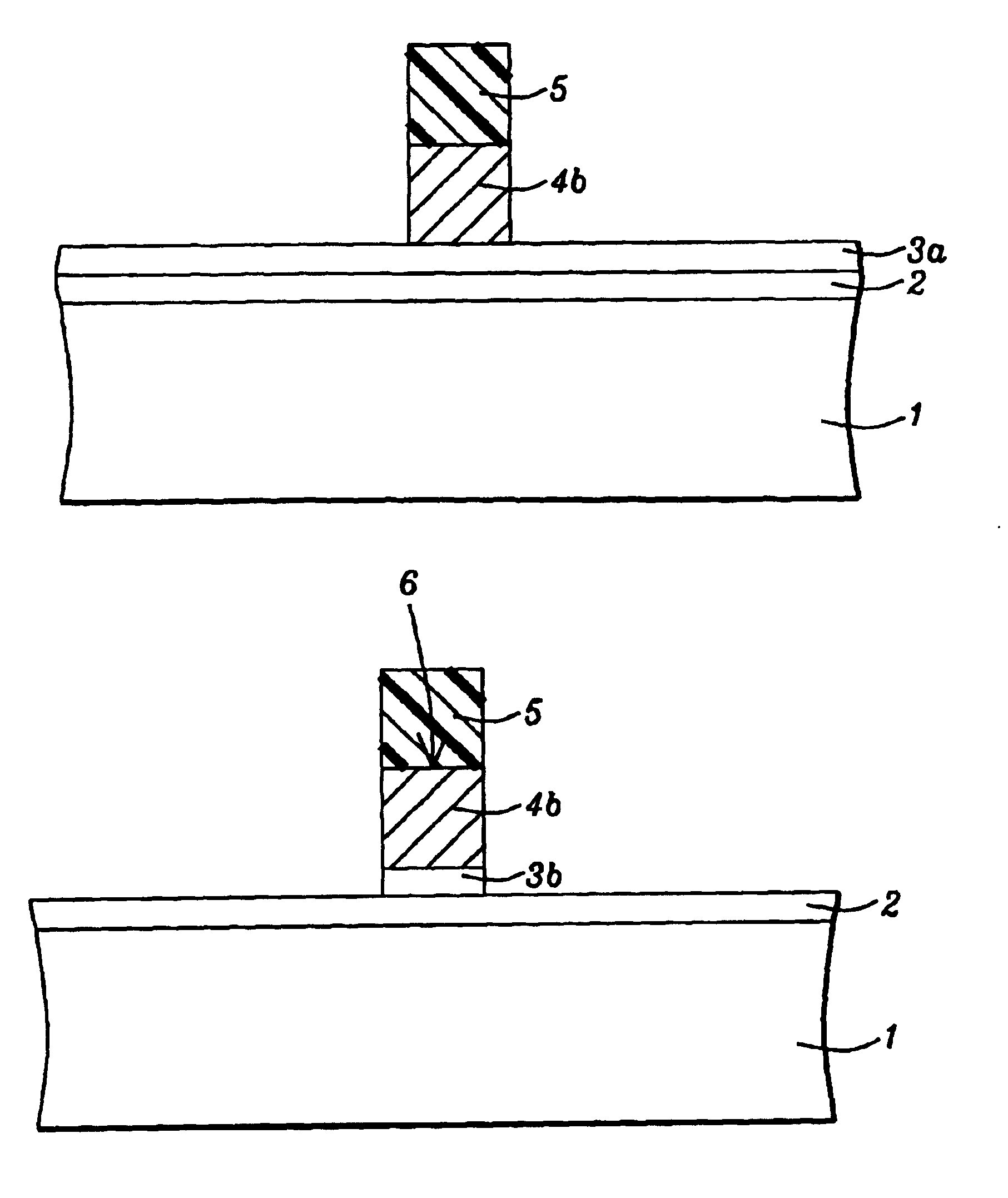
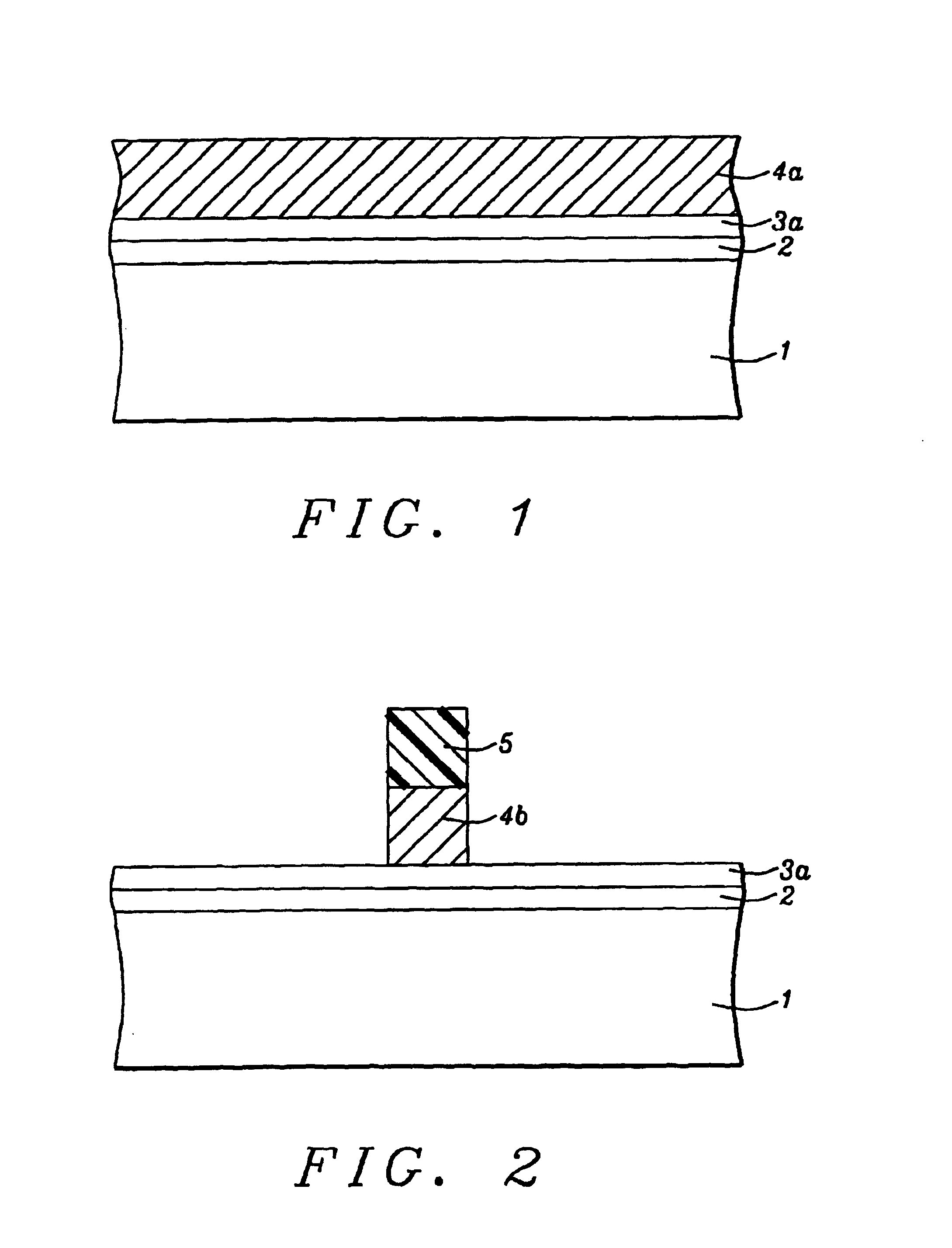
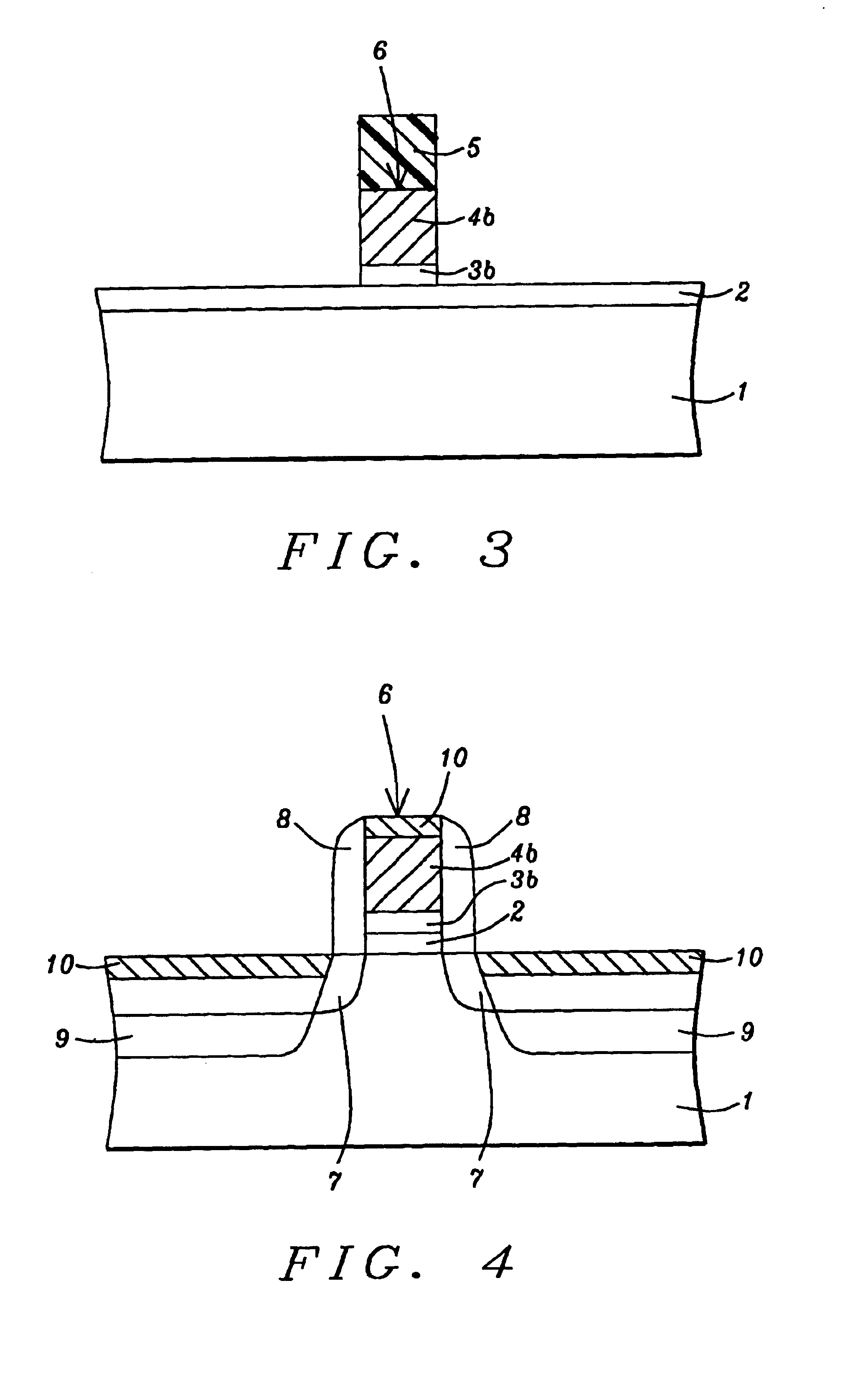
[0017]The method of forming a composite gate structure comprised of an overlying polysilicon component and a thin, underlying titanium nitride component, for use as gate structures for conventional planar type MOSFET or CMOS devices, as well as for fin type field effect transistor (FINFET), or a vertical double gate devices, will now be described in detail. A first iteration of this invention entails the use of P type, semiconductor substrate 1, comprised of single crystalline silicon featuring a crystallographic orientation. Gate insulator layer 2, comprised of silicon dioxide is next thermally grown to a thickness between about 8 to 40 Angstroms. If desired high dielectric constant layers, such as HfO2, ZrO2, and SiN, can be used as gate insulator layers. Conductive layer 3a, needed for the underlying component of a composite gate structure, is next deposited via physical vapor deposition procedures to a thickness between about 10 to 300 Angstroms. A conductive layer with a speci...


PUM


Abstract

A method of forming a composite gate structure for a planar MOSFET device, as well as for vertical, double gate, FINFET device, has been developed. The method features a composite gate structure comprised of an overlying silicon gate structure shape, and an underlying titanium nitride gate structure shape. The titanium nitride component allows a lower work function, and thus lower device operating voltages to be realized when compared to counterpart gate structures formed with only polysilicon. A novel, two step gate structure definition procedure, featuring an anisotropic first etch procedure for definition of the polysilicon gate structure shape, followed by a wet or dry isotopic second etch procedure for definition of the titanium nitride gate structure shape, is employed.

Description

BACKGROUND OF THE INVENTION[0002](1) Field of the Invention[0003]The present invention relates to methods used to fabricate semiconductor devices, and more specifically to a method used to form a gate structure for a metal oxide semiconductor field effect transistor (MOSFET), or complimentary metal oxide semiconductor (CMOS), device.[0004](2) Description of Prior Art[0005]Specific properties of polysilicon, such as the ability to withstand self-aligned metal silicide procedures, have resulted in the extensive use of polysilicon as a material for a gate structure for CMOS devices. However other characteristics of polysilicon can adversely influence the use of polysilicon gate structures for sub-100 um CMOS applications. For example the need to use low operating conditions for present CMOS applications demand devices featuring controllable, low threshold voltage. To establish low threshold voltages the work function of the gate structure should be lower than the work function obtained...

Claims


Application Information

Patent Timeline
IPC IPC(8): H01L29/786H01L21/02H01L29/423H01L29/66H01L21/336H01L29/40H01L29/49H01L21/28
CPCH01L29/42384H01L29/785H01L29/66795H01L29/4966H01L21/28088H01L29/665
Inventor CHIU, HSIEN-KUANGCHEN, FANG-CHENGCHEN, HAUR-YWHTAO, HUN-JANCHIU, YUAN-HUNG
Owner TAIWAN SEMICON MFG CO LTD
Why Eureka
Try Eureka