Eureka AIR delivers breakthrough ideas for toughest innovation challenges, trusted by R&D personnel around the world.

Sequencer and method of selectively inhibiting clock signals to execute reduced instruction sequences in a re-programmable I/O interface

Inactive Publication Date: 2005-03-22
CONEXANT
View PDF13 Cites 18 Cited by
  • Summary
  • Abstract
  • Description
  • Claims
  • Application Information

AI Technical Summary

Benefits of technology

The present invention has resulted, in significant part, from the discovery and recognition that a very substantial amount of I / O signal processing can be performed with a serial interface using a small set of relatively powerful, special purpose instructions and a reduced frequency of the clock used to execute those instructions. No more than two instructions need be executed for each time period during which bit signals are communicated to or from the interface. Many instructions provide the ability to perform multiple functions simultaneously, and the opportunity to execute two of these instructions during each time period of bit signal transmission and reception permits the opportunity to set up the necessary functionality in the interface for the transmission and / or reception of the bit signals and ancillary clock and control signals as may be necessary.
Of course, executing the instructions at reduced clock frequency reduces the amount of power consumed, because the power consumption is directly related to the clock frequency. Reducing the size and number of the instructions has the effect of reducing the size of the modules required to implement the interface, thereby facilitating its integration into a system on a chip or other ASSPs. The implementation of the interface is also directly enhanced by using digital logic circuit elements which minimize or avoid extra time clocks and time delays, while still minimizing the size of the interface.
The present invention also recognizes and resolves the issue of making short haul serial peripheral interfaces reprogrammable. Being re-programmable, each interface may be changed in functionality to implement different serial bus protocols by simply loading new instructions required for the protocols. Reprogrammability permits a range of generalities to be implemented in a system chip with an embedded processor, because the interface can be reprogrammed to implement any of the inter-chip serial bus protocols without restricting the bus protocol to a single hard wired implementation. Thus the previous restriction of using controllers and other system chips with only a single serial peripheral bus protocol is eliminated, which offers the advantage of allowing the user to select the most effective bus communication protocol for the elements within and exterior of the system chip. Avoiding this restriction permits the same system chip to execute different re-programmable firmware to support a variety of different serial bus protocols, allowing the functionality of the system chip to be updated with advancements in communication protocols.

Problems solved by technology

Of course, executing the instructions at reduced clock frequency reduces the amount of power consumed, because the power consumption is directly related to the clock frequency.

Method used


Image

  • Sequencer and method of selectively inhibiting clock signals to execute reduced instruction sequences in a re-programmable I/O interface
  • Sequencer and method of selectively inhibiting clock signals to execute reduced instruction sequences in a re-programmable I/O interface
  • Sequencer and method of selectively inhibiting clock signals to execute reduced instruction sequences in a re-programmable I/O interface

Examples


Embodiment Construction

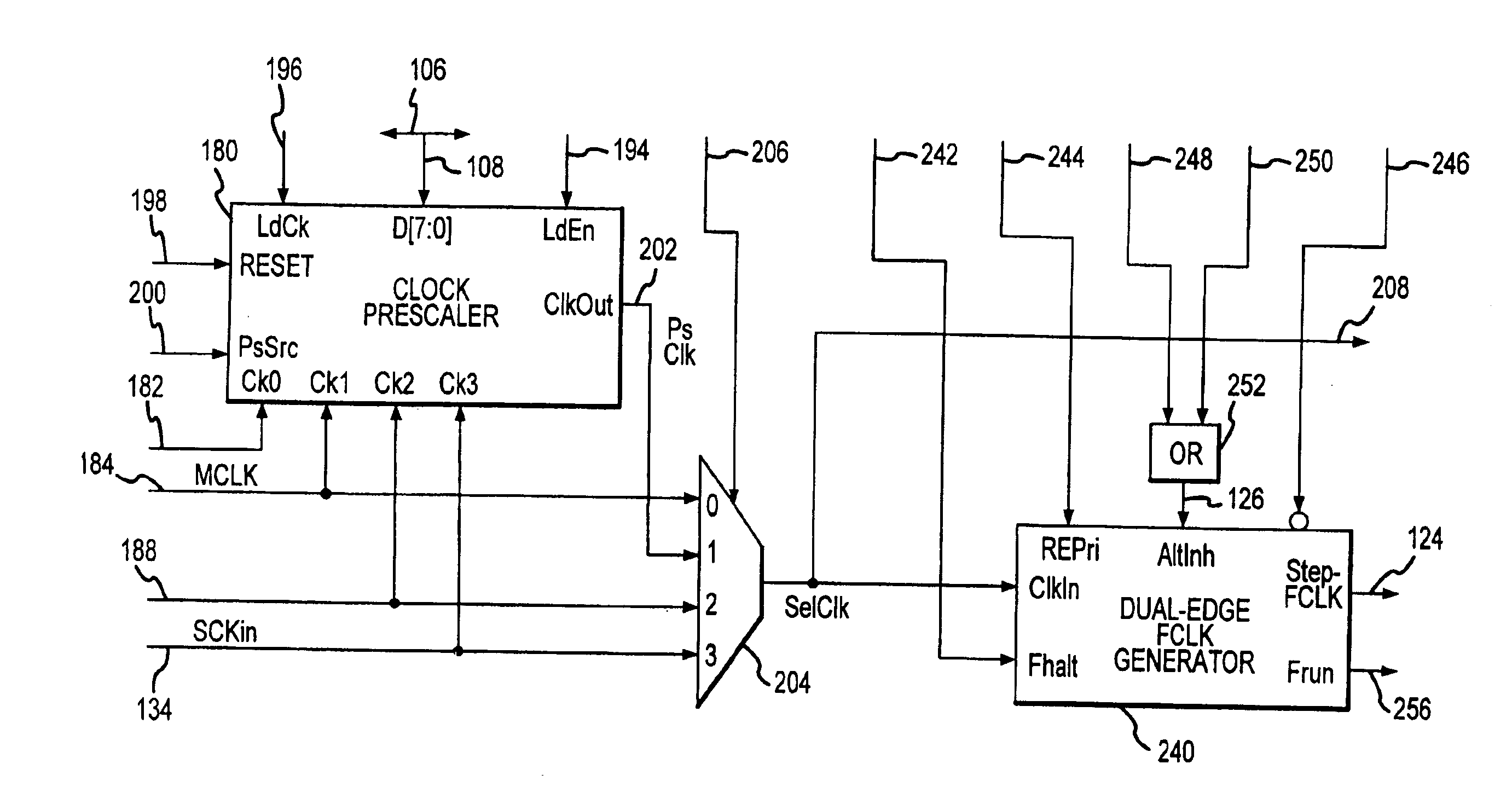
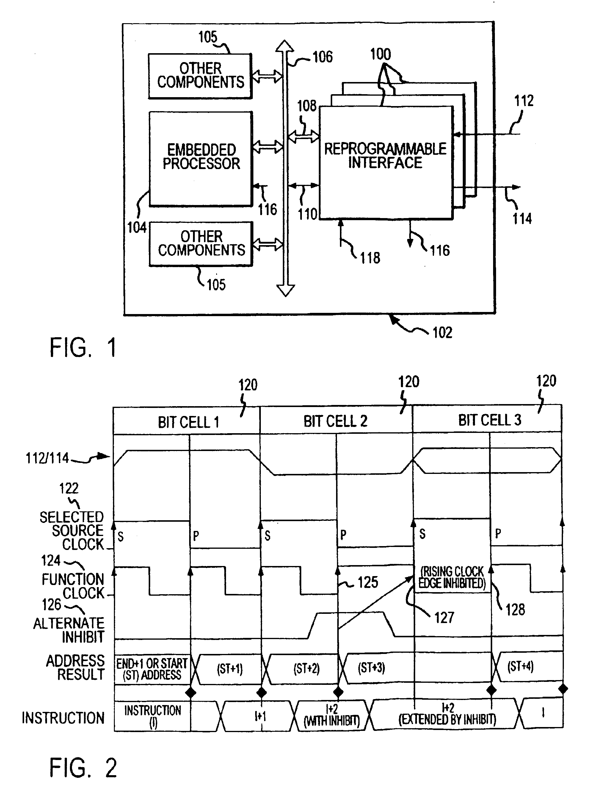
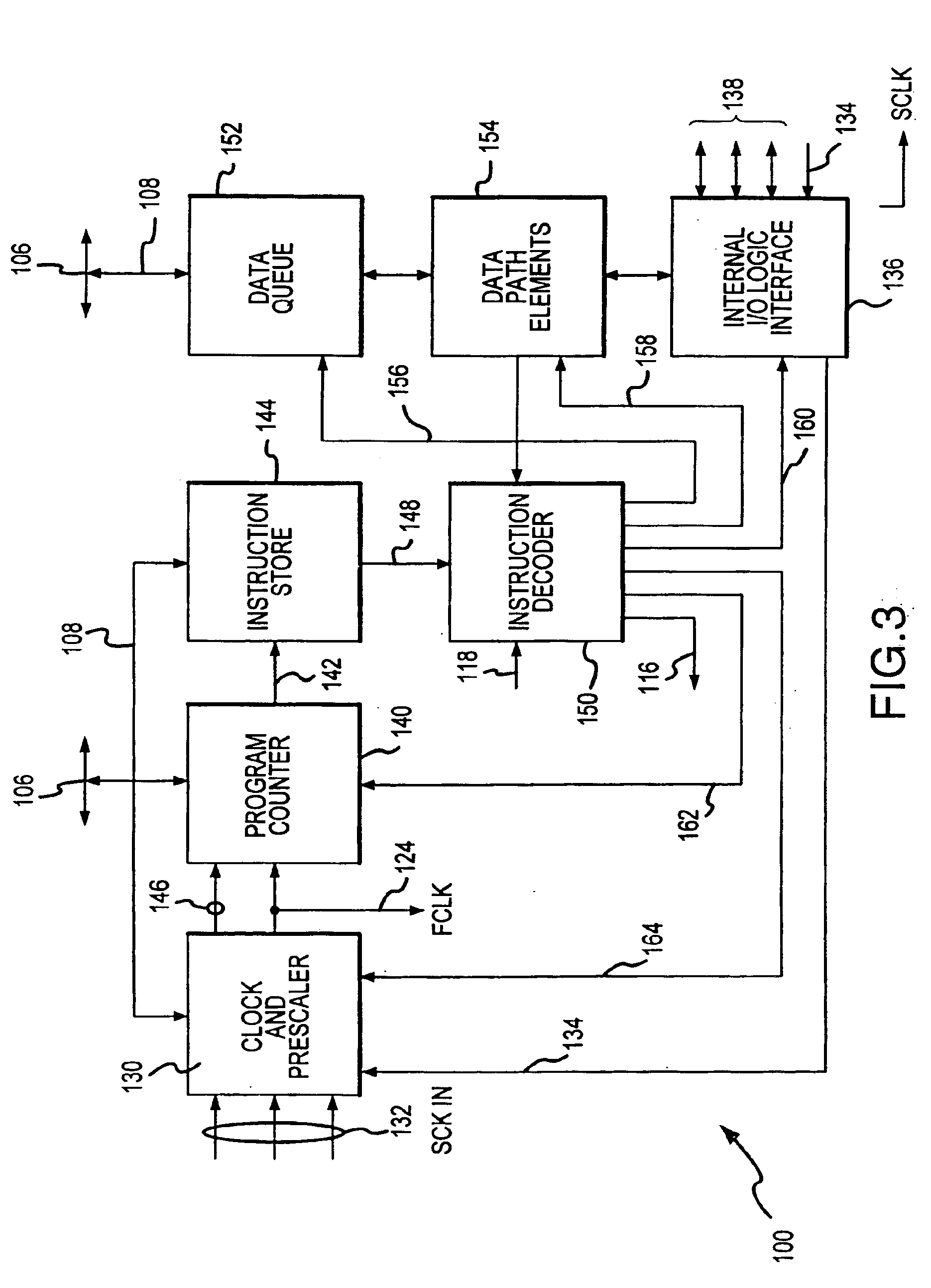
A reprogrammable interface 100, in which the present invention is embodied, is preferably a part of a larger system on a chip or system chip 102, such as an ASSP, as shown in FIG. 1. In addition to the reprogrammable interface100, the system chip 102 includes an embedded controller or processor 104 and other components 105, such as memory, which are specific to the system chip 102. Preferably, the system chip 102 will also include one or more of the reprogrammable interfaces 100. An internal bus 106 connects each reprogrammable interface 100, the embedded processor 104 and the other on-chip modules 105 together, by which signals are communicated between these elements. The reprogrammable functionality of the interface 100 is achieved as a result of the processor 104 loading different sets of code or values which define instructions into the interface 100. The code or instructions are loaded into the interface 100 over data lines 108 which extend from the internal bus 106. Control an...


PUM


Abstract

A sequencer executes instructions based on a function clock signal to perform I / O functions in a serial peripheral interface based on a source clock signal. The function clock signal has a frequency of two times the frequency of the source clock signal. A function clock generator generates the function clock signal and operatively selects the instruction to be decoded. The instruction selectively forces the frequency of the function clock signal to be equal to the frequency of the source clock signal during the duration of that function clock signal during which the predetermined instruction is decoded to execute a single instruction during the source clock signal, to advantageously repeat the execution of the instruction without consuming clock cycles.

Description

FIELD OF THE INVENTIONThis invention relates to input / output (I / O) interfaces used for connecting relatively complex and high capacity computer systems to peripheral equipment. More particularly, the present invention relates to a new and improved I / O interface by which to send and receive communication signals, preferably in a serial or narrow parallel form, which offers the advantage of relatively small size, relatively high performance, relatively low power consumption, and comparatively great versatility and flexibility in accommodating and executing a variety of different complex communication protocols.BACKGROUND OF THE INVENTIONMany modern electronic devices are built as an entire system on a single semiconductor chip, and as such, are known as system on a chip (SoC) integrated circuits or application specific standard products (ASSPs). Building an entire system or large portion of the system on a single chip has a number of advantages. Although the costs of initially designi...

Claims


Application Information

Patent Timeline
IPC IPC(8): G06F9/38G06F9/308G06F9/32G06F9/30
CPCG06F9/30018G06F9/30069G06F9/3869G06F9/325G06F9/30079
Inventor FISCHER, MICHAEL A.
Owner CONEXANT
Why Eureka
Eureka Blog
Learn More