Method of manufacturing a semiconductor device

Inactive Publication Date: 2005-03-29
SEMICON ENERGY LAB CO LTD
View PDF88 Cites 40 Cited by
  • Summary
  • Abstract
  • Description
  • Claims
  • Application Information

AI Technical Summary

Benefits of technology

The present invention has been made in view of the above and an object of the present invention is therefore to provide a method in which an amorphous semiconductor film is annealed with an excimer laser and then further subjected to laser annealing by a second

Problems solved by technology

This is the cause of fluctuation in grain size.
It is thus impossible to obtain a desirable electric charact

Method used


Image

  • Method of manufacturing a semiconductor device
  • Method of manufacturing a semiconductor device
  • Method of manufacturing a semiconductor device

Examples


Example

Embodiment 1 will describe a case in which an amorphous silicon film is formed by a sputtering apparatus and the film is subjected to laser annealing using an XeCl excimer laser and a YAG laser.

A 5 inch square Corning 1737 substrate with a thickness of 0.7 mm is prepared. A silicon oxynitride film with a thickness of 200 nm is formed on the substrate by using a plasma CVD apparatus. Then a sputtering apparatus is used to form an amorphous silicon film on the surface of the silicon oxynitride film to a thickness of 50 nm.

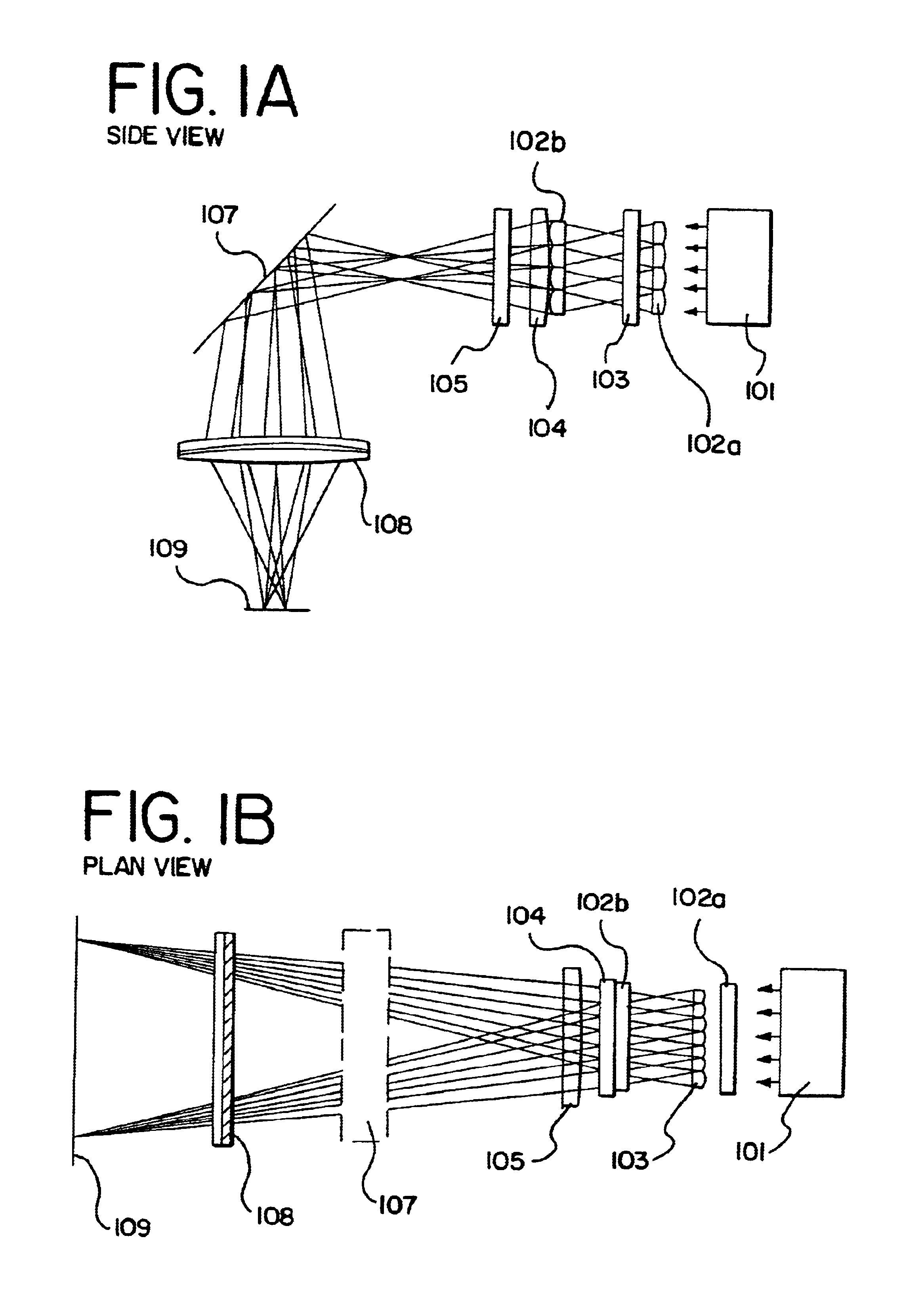
Thereafter, the XeCl excimer laser L3308 (wavelength: 308 nm, pulse width: 30 ns) manufactured by Lamda Physik, Inc. is used for laser annealing. This laser emitter emits a pulse oscillation laser and is capable of outputting an energy of 500 mJ / pulse. The size of the laser beam is 10×30 mm (both are half-width in the beam profile) at its exit. The laser beam emitted from the XeCl excimer laser is processed by an optical system as the one shown in FIGS. 1A and 1B int...

Example

Embodiment 2

A description given in Embodiment 2 is a case in which an amorphous silicon film is formed by a CVD apparatus and then subjected to heat treatment followed by laser annealing using an XeCl excimer laser and a second harmonic of a YAG laser.

A 5 inch square Corning 1737 substrate with a thickness of 0.7 mm is prepared. A silicon oxynitride film with a thickness of 200 nm is formed on the substrate by using a plasma CVD apparatus. Subsequently the same plasma CVD apparatus is used to form an amorphous silicon film on the surface of the silicon oxynitride film to a thickness of 50 nm. A solution containing an element that promotes crystallization is applied to the amorphous silicon film. When a nickel acetate solution, for instance, is used as the applied solution, the entire surface of the film is coated with the nickel acetate solution (with a weight percent of 10 ppm) by spin coating.

Next, the substrate is heated in nitrogen atmosphere at a temperature of 500° C. for an h...

Example

Embodiment 3 gives a description of a case where heat treatment is conducted before laser annealing using a KrF excimer laser and a second harmonic of a YAG laser.

Through the same method as Embodiment 2, a silicon oxynitride film and an amorphous silicon film are formed and the amorphous silicon film is coated with a solution containing an element that promotes crystallization. Then the substrate is heated in nitrogen atmosphere at a temperature of 500° C. for an hour and further heated in nitrogen atmosphere at 550° C. for four hours.

Thereafter, the substrate is annealed with a KrF excimer laser having a wavelength of 248 nm by using an optical system as the one shown in FIGS. 1A and 1B. From FIG. 3, it is found that the absorption coefficient of a KrF excimer laser whose wavelength is 248 nm is 1.64×106 cm−1 and 1.86×106 cm−1 for an amorphous silicon film and for a polycrystalline silicon film, respectively. Therefore a KrF excimer laser is absorbed in an amorphous silicon film an...


PUM

PropertyMeasurementUnit
Nanoscale particle sizeaaaaaaaaaa
Wavelengthaaaaaaaaaa

Abstract

By using lasers having different wavelengths in laser annealing of an amorphous semiconductor film, the amorphous semiconductor film can be crystallized and the crystallinity of the crystallized film is improved. A laser 126 to 370 nm in wavelength is used first to subject an amorphous semiconductor film to laser annealing, thereby obtaining a crystalline semiconductor film. In desirable laser annealing, a subject surface is irradiated with a laser beam processed by an optical system into a linear laser beam that is linear in section on the subject surface. Next, a laser 370 to 650 nm in wavelength is used to irradiate the above crystalline semiconductor film by again processing the laser beam into a linear beam through an optical system. A crystalline semiconductor film thus obtained has an excellent crystallinity. If this crystalline semiconductor film is used to form an active layer of a TFT, an electric characteristic of the TFT can be improved.

Description

BACKGROUND OF THE INVENTION1. Field of the InventionThe present invention relates to a method of manufacturing a semiconductor device having a circuit that is composed of a thin film transistor (hereinafter referred to as TFT). For instance, the invention relates to an electro-optical device represented by a liquid crystal display device and to electric equipment having an electro-optical device as its component. Note that the term semiconductor device herein refers to a device in general which functions through utilization of semiconductor characteristics, and that the above electro-optical device and electric equipment fall into this category.2. Description of the Related ArtIn recent years, voluminous research has been made on a laser annealing technique for crystallizing an amorphous semiconductor film formed on an insulating substrate made of glass or the like, or for improving crystallinity of a partially crystallized semiconductor film. The amorphous semiconductor film is oft...

Claims


Application Information

Patent Timeline
IPC IPC(8): H01L21/70H01L21/20H01L21/02H01L29/66H01L27/12H01L21/336H01L29/786H01L21/84H01L21/77
CPCH01L21/2026H01L27/12H01L29/66757H01L27/1285H01L29/78636H01L27/124H01L29/78621H01L29/42384H01L29/458H01L29/78645H01L2029/7863H01L21/0262H01L21/02686H01L21/02683H01L21/02502H01L21/02678H01L21/02488H01L21/02422H01L21/02532H01L21/02672H01L21/02691H01L21/02675
Inventor TANAKA, KOICHIRO
Owner SEMICON ENERGY LAB CO LTD
Why Eureka
Try Eureka