Semiconductor device

Inactive Publication Date: 2005-03-29
MICRON TECH INC
View PDF209 Cites 79 Cited by
  • Summary
  • Abstract
  • Description
  • Claims
  • Application Information

AI Technical Summary

Benefits of technology

According to an aspect of the present invention, there is provided a semiconductor device comprising:a substrate:at least one data storage cell provided on one side of said substrate, wherein the or each said data storage cell comprises a respective field effect transistor comprising (i) a source; (ii) a drain; (iii) a body arranged between said source and said drain and adapted to at least temporarily retain a net electrical charge generated in said body such that the magnitude of said net charge can be adjusted by input signals applied to said transistor; and (iv) at least one gate adjacent said body; and charge adjusting means for at least partially cancelling the adjustment of said net electrical charge by said input signals, by applying first predetermined electrical voltage signals between at least one corresponding said gate and the corresponding said drain and between the corresponding said source and said drain. The present invention is ba

Problems solved by technology

SOI technology suffers the drawback that because the body region of each individual transistor is electrically insulated from the underlying silicon substrate, electrical charging of the body can occur under certain conditions.
This can have an effect on the electrical performance of the transistors and is generally regarded as an undesirable effect.
This known device suffers from the drawback that it requires at least four terminal connections for its operation (connected to the drain, gate, source and impurity region of opposite polarity or to the substrate), which increases the complexity of the device.
Furtherm

Method used


Image

  • Semiconductor device
  • Semiconductor device
  • Semiconductor device

Examples


Example

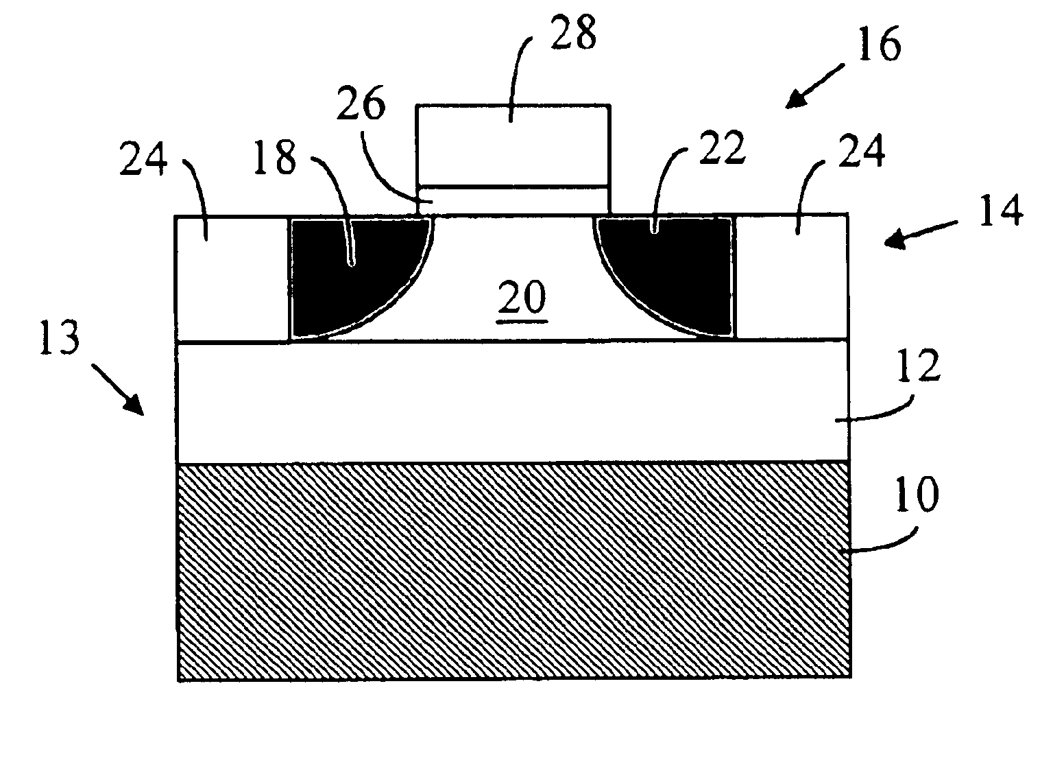
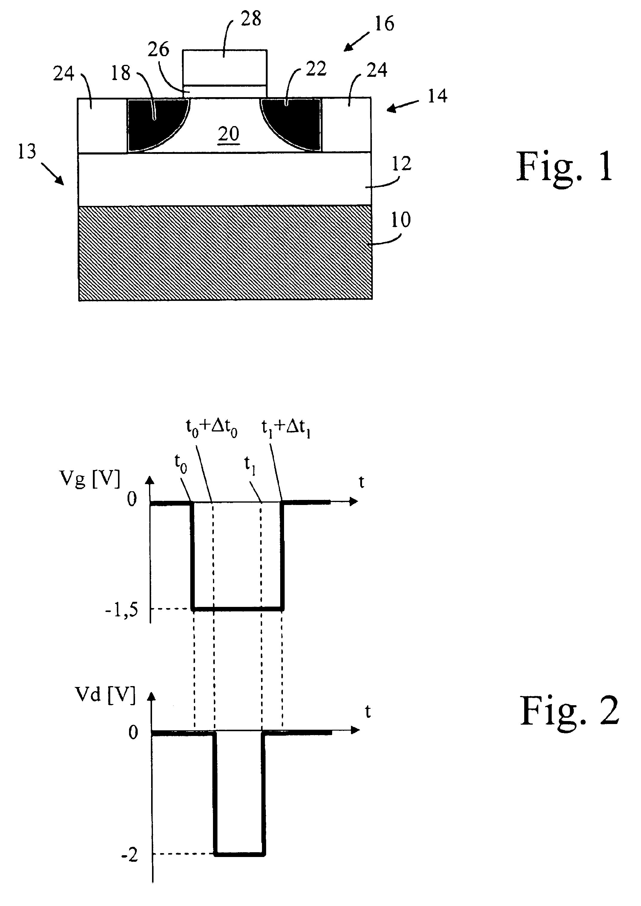
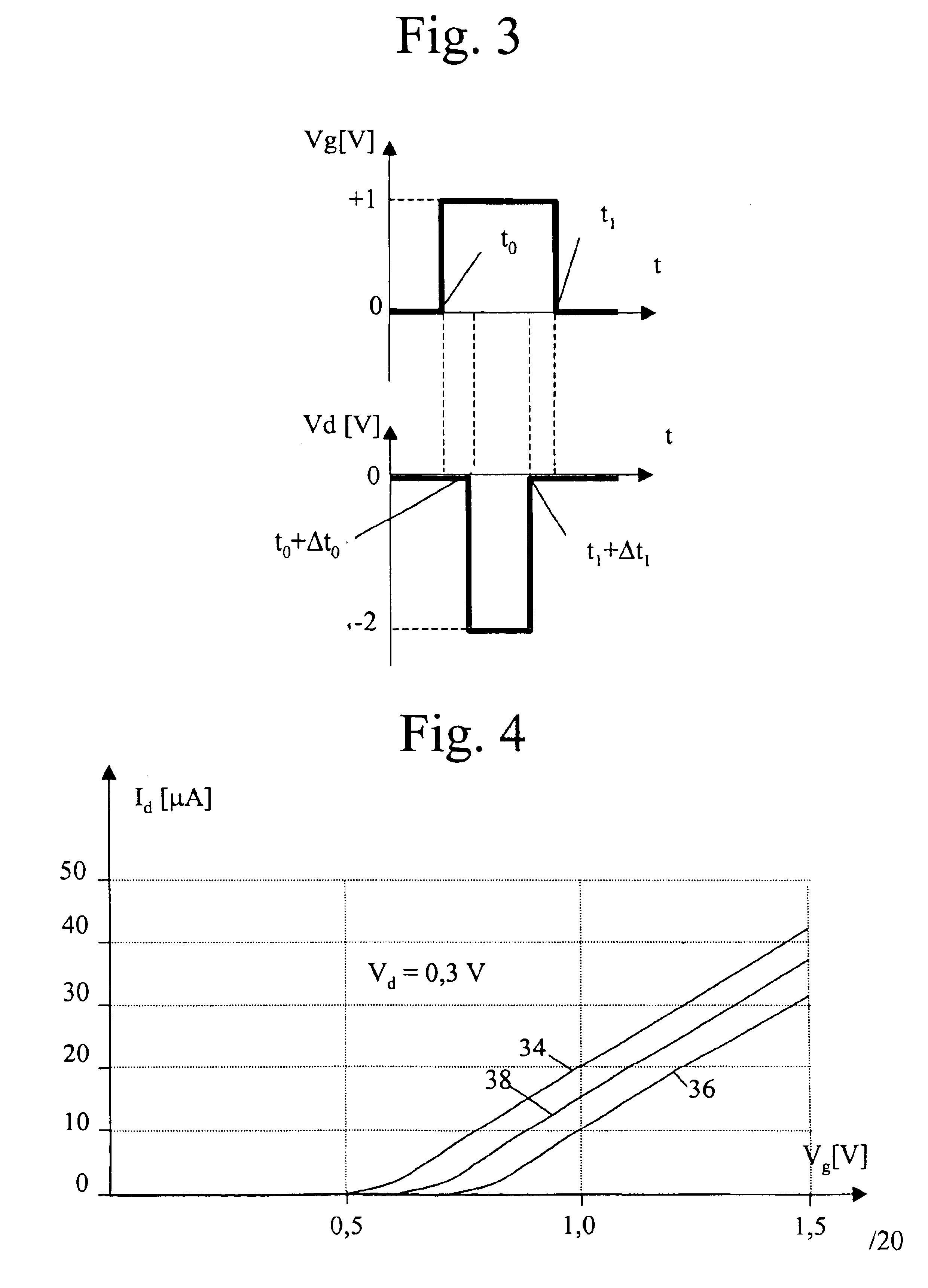
Referring firstly to FIG. 1, an NMOS SOI (silicon on insulator) MOSFET (metal-oxide-silicon field effect transistor) comprises a silicon wafer 10 coated with a layer 12 of silicon dioxide, the wafer 10 and layer 12 constituting a substrate 13. A layer 14 formed on the substrate 13 consists of an island 16 of silicon doped with impurities to form a source 18 on n-type material, a body 20 of p-type material and a drain 22 of n-type material, together with a honeycomb insulating structure 24 of silicon dioxide, the honeycomb structure being filled by a plurality of islands 16. The source 18 and drain 22 extend through the entire thickness of the silicon layer 14. An insulating film 26 is formed over body 20, and a gate 28 of doped semiconductor material is provided on dielectric film 26. The production process steps, chemical compositions and doping conditions used in manufacturing the transistor of FIG. 1 will be familiar to persons skilled in the art, and are also described in furthe...


PUM


Abstract

A semiconductor device, such as a memory device or radiation detector, is disclosed, in which data storage cells are formed on a substrate. Each of the data storage cells includes a field effect transistor having a source, drain, and gate, and a body arranged between the source and drain for storing electrical charge generated in the body. The magnitude of the net electrical charge in the body can be adjusted by input signals applied to the transistor, and the adjustment of the net electrical charge by the input signals can be at least partially cancelled by applying electrical voltage signals between the gate and the drain and between the source and the drain.

Description

BACKGROUNDThe present invention relates to semiconductor devices, and relates particularly, but not exclusively, to DRAM memory devices using SOI (silicon on insulator) technology.DRAM memories are known in which each memory cell consists of a single transistor and a single capacitor, the binary 1's and 0's of data stored in the DRAM being represented by the capacitor of each cell being in a charged or discharged state. Charging and discharging of the capacitors is controlled by switching of the corresponding transistor, which also controls reading of the data stored in the cell. Such an arrangement is disclosed in U.S. Pat. 3,387,286 and will be familiar to persons skilled in the art.Semiconductor devices incorporating MOSFET (metal oxide semiconductor field effect transistor) type devices are well known, and arrangements employing SOI (silicon on insulator) are becoming increasingly available. SOI technology involves the provision of a silicon substrate carrying an insulating sili...

Claims


Application Information

Patent Timeline
IPC IPC(8): G11C11/404G11C11/403G01T1/24H01L21/8242H01L27/108H01L29/786H01L31/10
CPCG11C11/403G11C11/404G11C11/5621H01L21/84H01L27/108H01L27/10844H01L27/1203H01L29/7841H01L27/10802G11C2211/4016Y10S438/982Y10S257/905Y10S257/907H10B12/20H10B12/01H10B12/00H04N25/772
Inventor FAZAN, PIERREOKHONIN, SERGUEI
Owner MICRON TECH INC
Why Eureka
Try Eureka