Process for production of SOI substrate and process for production of semiconductor device

a technology of soi substrate and semiconductor device, which is applied in the direction of semiconductor devices, radio frequency controlled devices, electrical devices, etc., can solve the problems of single-crystal silicon thin film cracking and peeling at the edges of silicon substrate, stress to occur,

Inactive Publication Date: 2005-04-05
SEMICON ENERGY LAB CO LTD
View PDF12 Cites 208 Cited by
  • Summary
  • Abstract
  • Description
  • Claims
  • Application Information

AI Technical Summary

Benefits of technology

The present invention was completed to address the above-mentioned problem. Thus, it is an object of the present invention to provide a process for producing a bonded SOI substrate without causing cracking and peeling to the thin film of single-crystal semiconductor.

Problems solved by technology

The disadvantage of this process is that the second heat treatment causes a strong stress to occur in the thin film of single-crystal silicon and this stress causes the thin film of single-crystal silicon to crack and peel at the edges of the silicon substrate.
This is a serious problem with “Smart-Cut” process, and an effective solution to it is required.

Method used


Image

  • Process for production of SOI substrate and process for production of semiconductor device
  • Process for production of SOI substrate and process for production of semiconductor device
  • Process for production of SOI substrate and process for production of semiconductor device

Examples


example 1

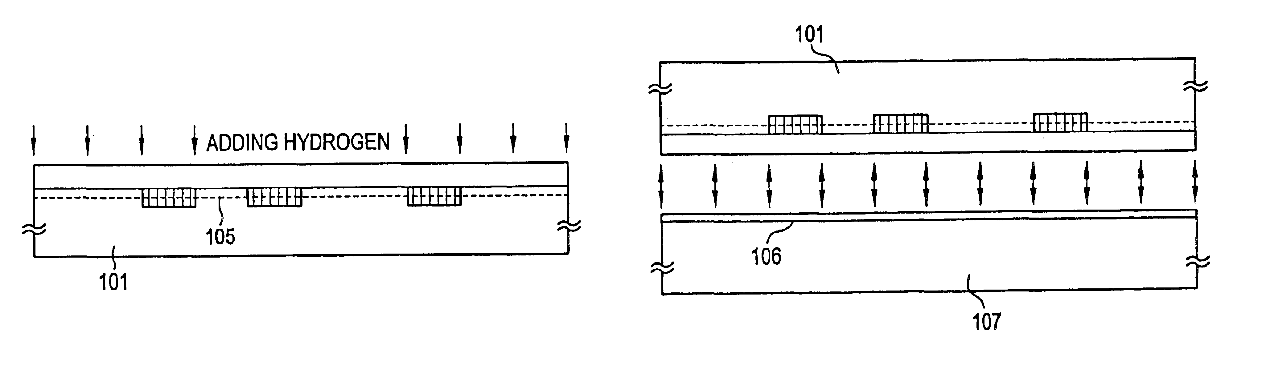
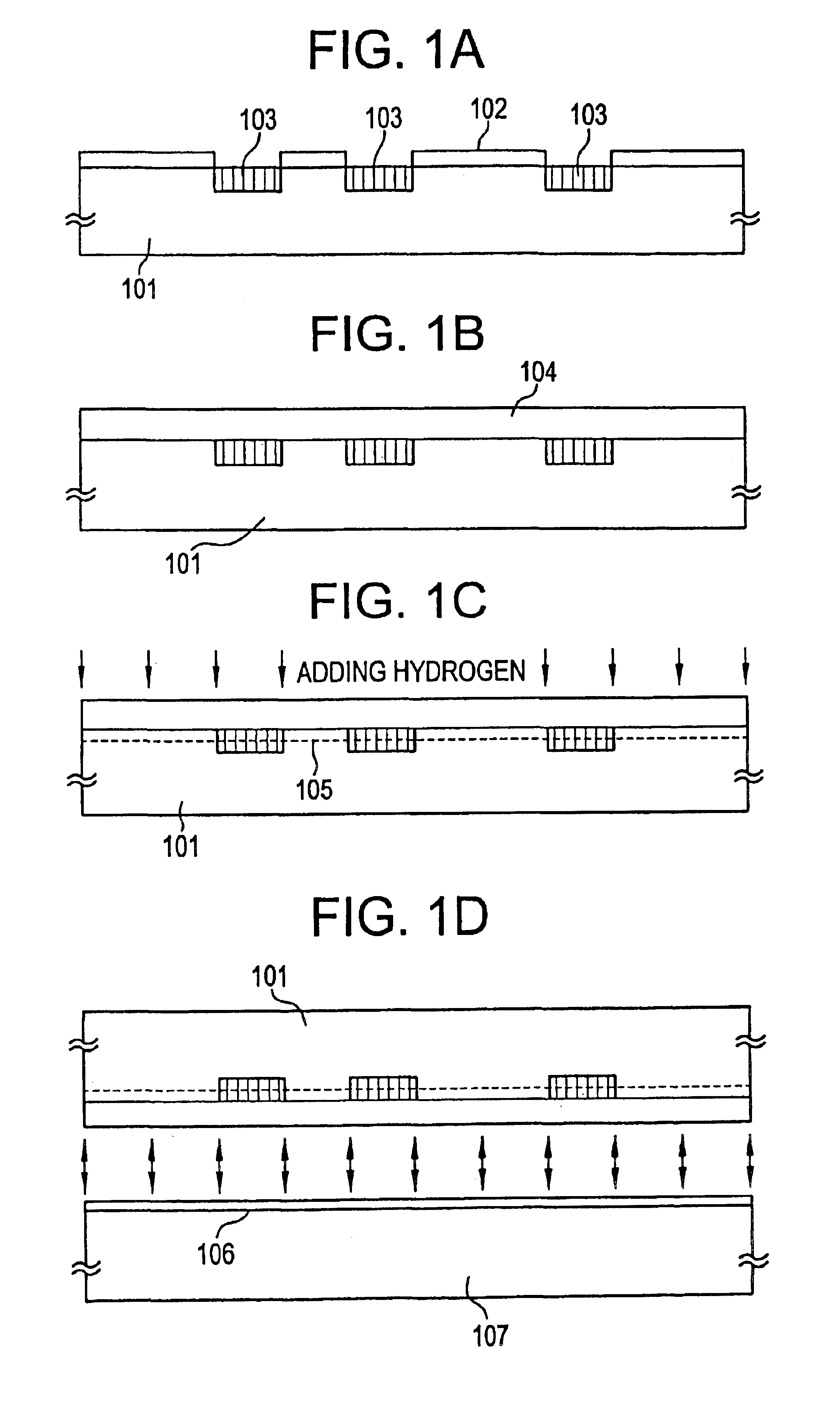
The process of the invention is explained with reference to FIGS. 1A to 1D and FIGS. 2A to 2C. First, a single-crystal silicon substrate 101 is made available. On its principal surface (on which elements are to be formed) is formed an insulating film, 50 nm thick, (which is a silicon oxide film in this example). The silicon oxide film is patterned to selectively form a mask 102. The silicon oxide film may be replaced by any other insulating film, such as silicon nitride film, silicon oxynitride film, and resist mask.

The mask 102 should cover the part which becomes the active layer of TFT afterward. Also the portion covered by the mask 102 may be used for thin film of single-crystal silicon.

The principal surface of the single-crystal silicon substrate 101 undergoes anodizing treatment, so that a portion of the single-crystal silicon substrate 101 (the exposed region without the mask 102) is converted into a porous silicon layer 103. This anodizing treatment may be carried out in a mi...

example 2

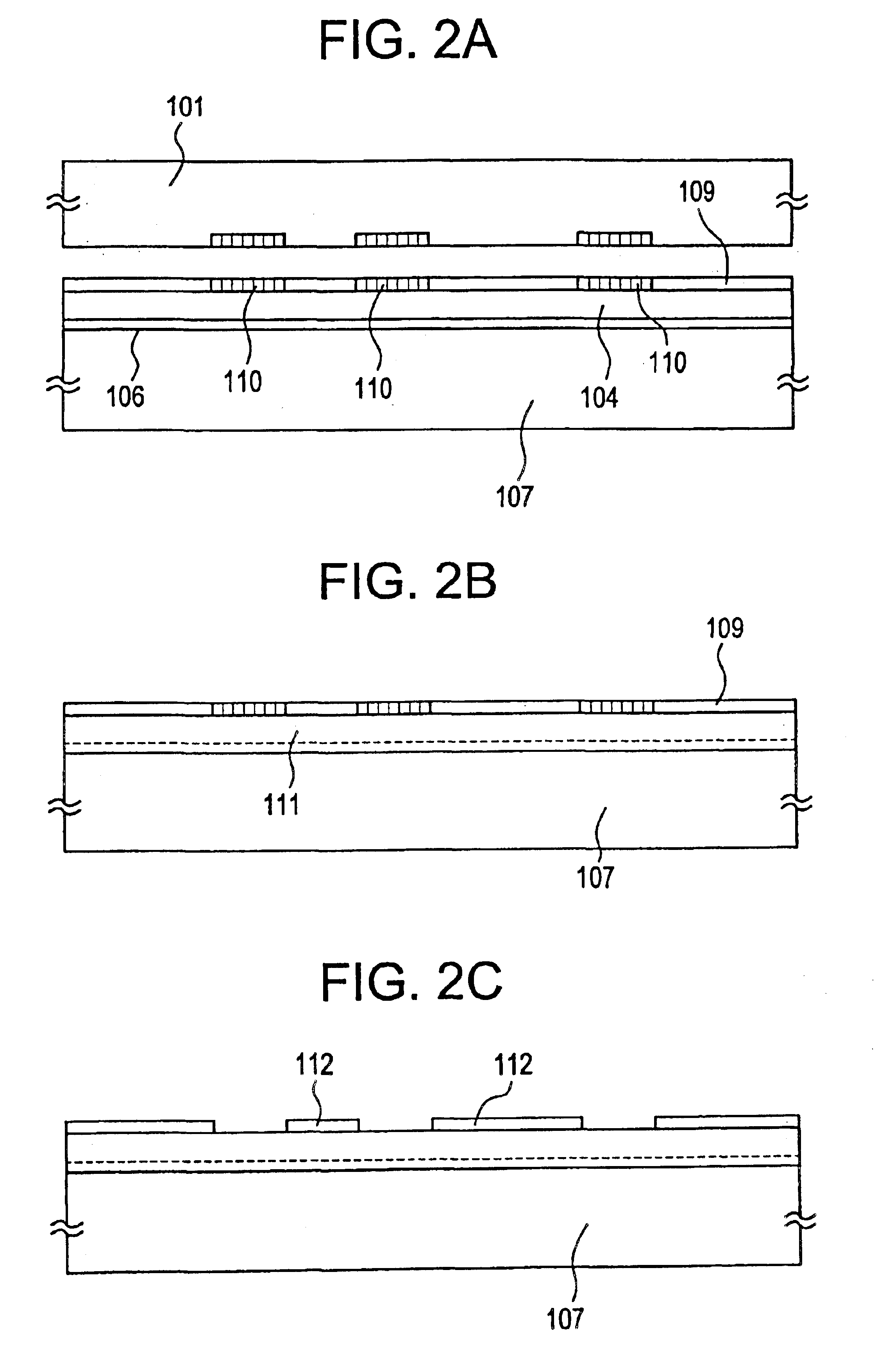
This example demonstrates, with reference to FIG. 3, the fabrication of TFT on the single-crystal silicon layer (in an island shape) which was formed by the process in Example 1.

First, the single-crystal silicon layer (in an island shape) is formed according to the process of Example 1. It is covered with a gate insulating film 302 of silicon oxide (120 nm thick) by plasma CVD. Then, a gate electrode 303 of n-type polysilicon is formed. See FIG. 3A.

Doping is performed to impart the n-type or p-type by the self-alignment process which employs the gate electrodes 303 as a mask. (In this example to fabricate n-type TFTs, the dopant is phosphorus. For p-type TFTs, the dopant is boron.) This step forms the impurity region 304. See FIG. 3B.

That part of the silicon layer which is just under the gate electrode may be doped with an impurity for reverse conductivity type (for example, boron in the case of n-type TFT) so as to control the threshold value of TFT. This doping may be accomplished...

example 3

This example demonstrates a liquid crystal display unit (FIG. 4) with TFT semiconductor circuits fabricated by the process in Example 2. The pixel TFT (or pixel switching element) and the cell assembly may be produced by any known method; therefore, their detailed description is omitted.

In FIG. 4, there are shown a supporting substrate (with an insulating surface) 11, a pixel matrix circuit 12, a source driver circuit 13, a gate driver circuit 14, a counter substrate 15, a FPC (flexible printed circuit) 16, and a signal processing circuit 17.

The signal processing circuit 17 contains such processing circuits as D / A converter, gamma-correcting circuit, and signal splitting circuit, which used to be formed in an IC. Signal processing may be accomplished by means of an IC chip (with MOSFETs conventionally fabricated on a single-crystal silicon substrate) on the supporting substrate.

Although this example demonstrates a liquid crystal display unit, the present invention may be applied to ...


PUM

PropertyMeasurementUnit
thickaaaaaaaaaa
thickaaaaaaaaaa
thickaaaaaaaaaa

Abstract

A process for producing an adhered SOI substrate without causing cracking and peeling of a single-crystal silicon thin film. The process consists of selectively forming a porous silicon layer in a single-crystal semiconductor substrate, adding hydrogen into the single-crystal semiconductor substrate to form a hydrogen-added layer, adhering the single-crystal semiconductor substrate to a supporting substrate, separating the single-crystal semiconductor substrate at the hydrogen-added layer by thermal annealing, performing thermal annealing again to stabilize the adhering interface, and selectively removing the porous silicon layer to give single-crystal silicon layer divided into islands.

Description

BACKGROUND OF THE INVENTION1. Field of the InventionThe present invention relates to a process for production of a thin-film transistor (TFT for short hereinafter) with single-crystal semiconductor thin film formed on a substrate having an insulating surface. The present invention relates also to a process for production of a semiconductor device containing semiconductor circuits constructed of TFTs.The term “semiconductor device” as used in this specification embraces any device that utilizes semiconductor characteristics for its functions. To be more specific, it includes electro-optical devices typified by liquid crystal displays, semiconductor circuits formed by integration of TFTs, and electronic machines and equipment containing as parts such electro-optical devices and semiconductor circuits.2. Description of the Relates ArtThe recent rapid progress in VLSI technology has yielded SOI (silicon on insulator) which is attracting attention because of its low power consumption. Th...

Claims


Application Information

Patent Timeline
Patent Type & Authority Patents(United States)
IPC IPC(8): H01L21/70H01L21/762H01L27/12H01L21/84H01L21/77H01L27/146H01L29/786
CPCH01L21/76254H01L27/1214H01L29/78621H01L27/1266H01L21/84Y10S438/96H01L27/146
Inventor FUKUNAGA, TAKESHI
Owner SEMICON ENERGY LAB CO LTD
Why Eureka
Try Eureka