Method for shifting the bandgap energy of a quantum well layer

a quantum well and bandgap energy technology, applied in the direction of lasers, nanooptics, semiconductor lasers, etc., can solve the problems of severe damage in the quantum well structure, atoms in the sample vibrating violently, point defects can move around in the crystal structure, etc., to reduce the formation of complex crystal defects, low implantation energy, and low implantation energy

Inactive Publication Date: 2005-04-12
HO SENG TIONG
View PDF18 Cites 18 Cited by
  • Summary
  • Abstract
  • Description
  • Claims
  • Application Information

AI Technical Summary

Benefits of technology

The inventive TAIVID process described herein reduces the formation of complex crystal defects in QW structures formed of, for example, III-V semiconductor materials by employing in-situ heating (i.e., an elevated temperature) to spread out the spatial distribution of the point defects created during an ion introduction (e.g., ion implantation) step.
An embodiment of the present invention provides a process for shifting the bandgap energy of a quantum well layer without inducing complex defects or generating significant free carriers. In addition, the process avoids the redistribution of dopants into the quantum well layer. The process includes introducing ions (e.g., deep level ion species) into a QW structure at an elevated temperature typically from about 200° C. to near the crystal damage temperature. The crystal damage temperatures can vary widely depending on the crystal materials. For InP / InGaAsP materials, the crystal damage temperature is at about 750° C. For GaAs / AlGaAs materials, the crystal damage temperature is at about 950° C. The QW structure includes an upper barrier layer, a lower barrier layer and a quantum well layer. The quantum well layer is disposed between the upper barrier layer and the lower barrier layer. The QW structure is then thermally annealed, thereby inducing quantum well intermixing (QWI) in the QW structure and shifting the bandgap energy of the quantum well layer.
In another aspect of the present invention, the in-situ sample heating is performed with the ions being implanted >0.5 μm away from a QW structure. This ion implantation condition is referred to as indirect-well implantation and the process is called Indirect-Well TAIVID (IDW TAIVID). The in-situ heating helps to drive-in the point defects towards the QW structure, which will allow the subsequent QWI to occur at a relatively low ion implantation dose even in the case where the QW structure is located at substantially away from the top wafer surface. The introduction of an implanted impurity >0.5 μm away from the QW structure helps to further reduce the formation of complex crystal defects at the quantum well that can cause damage to the active QW structure layers. Indirect-well implantation can be achieved with relatively low implantation energy so that low-energy implantation equipment can be used, which reduces the cost of the process. Thus, this process permits relatively low ion doses and low implantation energies to be used while still achieving the needed point defect concentration at the quantum well structure so that a high degree of intermixing or wavelength shift (˜100 nm or ˜60 meV) can occur during a subsequent annealing step.
Indirect-well implantation processes tend to have low spatial resolution as the ions spread (smear) out laterally when migrated to a QW structure. In as yet another aspect of the present invention, the in-situ sample heating is done with a patterned stress-inducing mask on a substrate (e.g., wafer) that includes a QW structure in order to achieve high spatial resolution for the subsequent QWI. The edges of the patterned stress-inducing mask cause material stress in the substrate and form stress field lines oriented in a direction perpendicular to the substrate surface (i.e., the vertical direction). These vertical stress field lines tend to limit the diffusion of point defects horizontally, since it is hard for the point defects to move across the vertical stress field lines. As a result, the vertical stress field reduce the lateral diffusion of point defects during ion implantation, thereby resulting in high spatial resolution for an area-selective wavelength shift.
In as yet another aspect of the present invention, the in-situ sample heating is performed with deep-level ion species, such as As, P, B, F, Xe, Ar and Ga. Deep-level species are not easy to ionize at room temperature and hence will not give rise to much free carriers in III-V semiconductor. This drastically reduces the concentration of free carriers in the material compared to shallow-level species such as Si, Zn, Be, Ge, Sn and S. The reduction of free carrier density with use of deep-level species reduces the optical loss in the waveguides. Thus this embodiment of the present invention provides a process for shifting the bandgap energy of a quantum well layer without inducing complex defects or generating significant free carriers.
In a process according to one exemplary embodiment of the present invention, the vacancy concentration generated during the ion introduction step (e.g., an ion implantation step) is maintained below the critical CDF concentration by performing the ion implantation at an elevated temperature. Performing the ion implantation with the quantum well structure at an elevated temperature results in thermal diffusion of the crystal site vacancies simultaneously with the generation of additional crystal site vacancies. The crystal site vacancies are, therefore, prevented from reaching the critical CDF concentration, even when ion doses of greater than 1×1015 cm−2 are employed.

Problems solved by technology

A point defect can move around in the crystal structure when the crystal structure is heated.
Heating can cause the atoms in the sample to vibrate violently.
The use of high-energy and / or high dose (i.e., a dose of greater than 1×1015 cm−2) ion implantation in conventional IID processes is known, however, to cause severe damage in the quantum well structure.
These drawbacks include difficulty in producing: (i) a low-loss waveguide photonic device due to free carrier absorption from implanted shallow-level ion species and scattering loss from complex defects induced by the IID process; (ii) photonic devices with controlled electrical characteristics (e.g., a desirable electrical conductivity or pn-junction properties) due to the aforementioned free carriers and complex defects, as well as due to re-distribution of dopants during the high temperature anneal step; and (iii) a photonic device with a high quality gain layer due to the IID process-induced complex defects, which create carrier recombination centers resulting in shorter carrier lifetime and lower optical gain.
The conventional ion implantation based IID processes do not adequately produce high quality photonic devices either in the form of single device or integrated multiple devices.
For example, conventional IID processes can achieve criteria (iii) and (iv), but have difficulty in satisfying criteria (i), (ii), (v) and (vi).

Method used


Image

  • Method for shifting the bandgap energy of a quantum well layer
  • Method for shifting the bandgap energy of a quantum well layer
  • Method for shifting the bandgap energy of a quantum well layer

Examples


Embodiment Construction

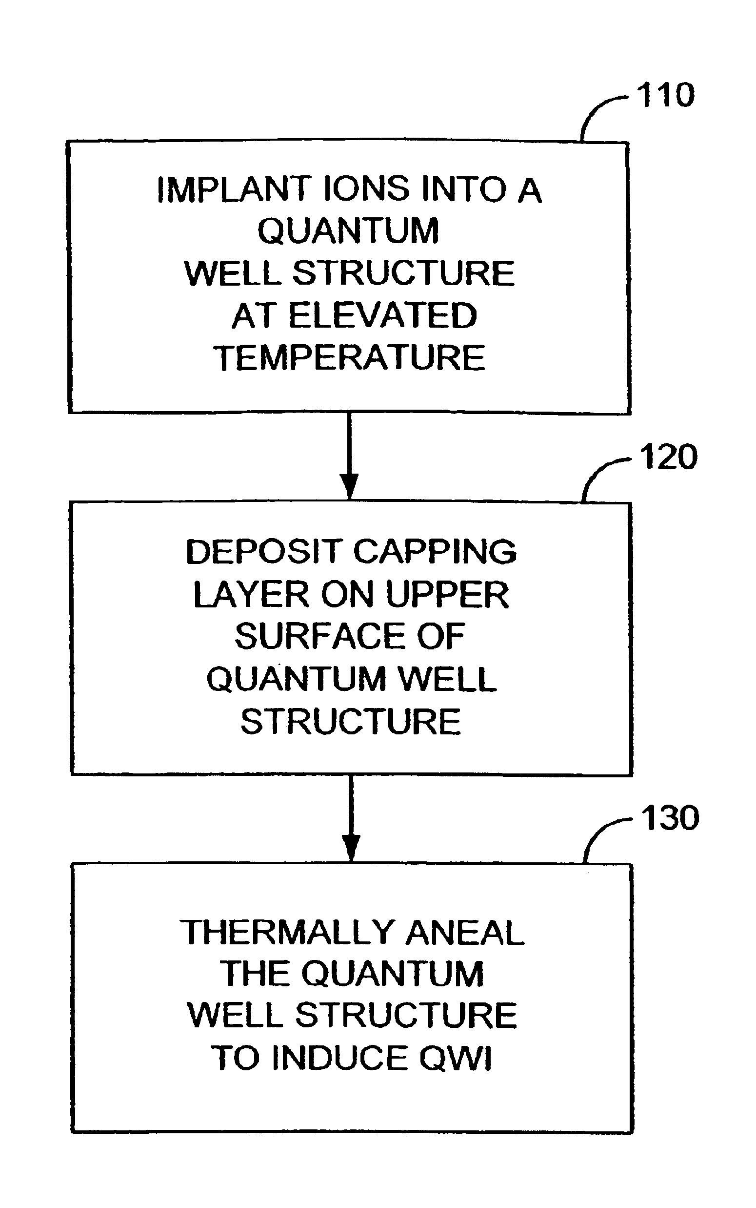
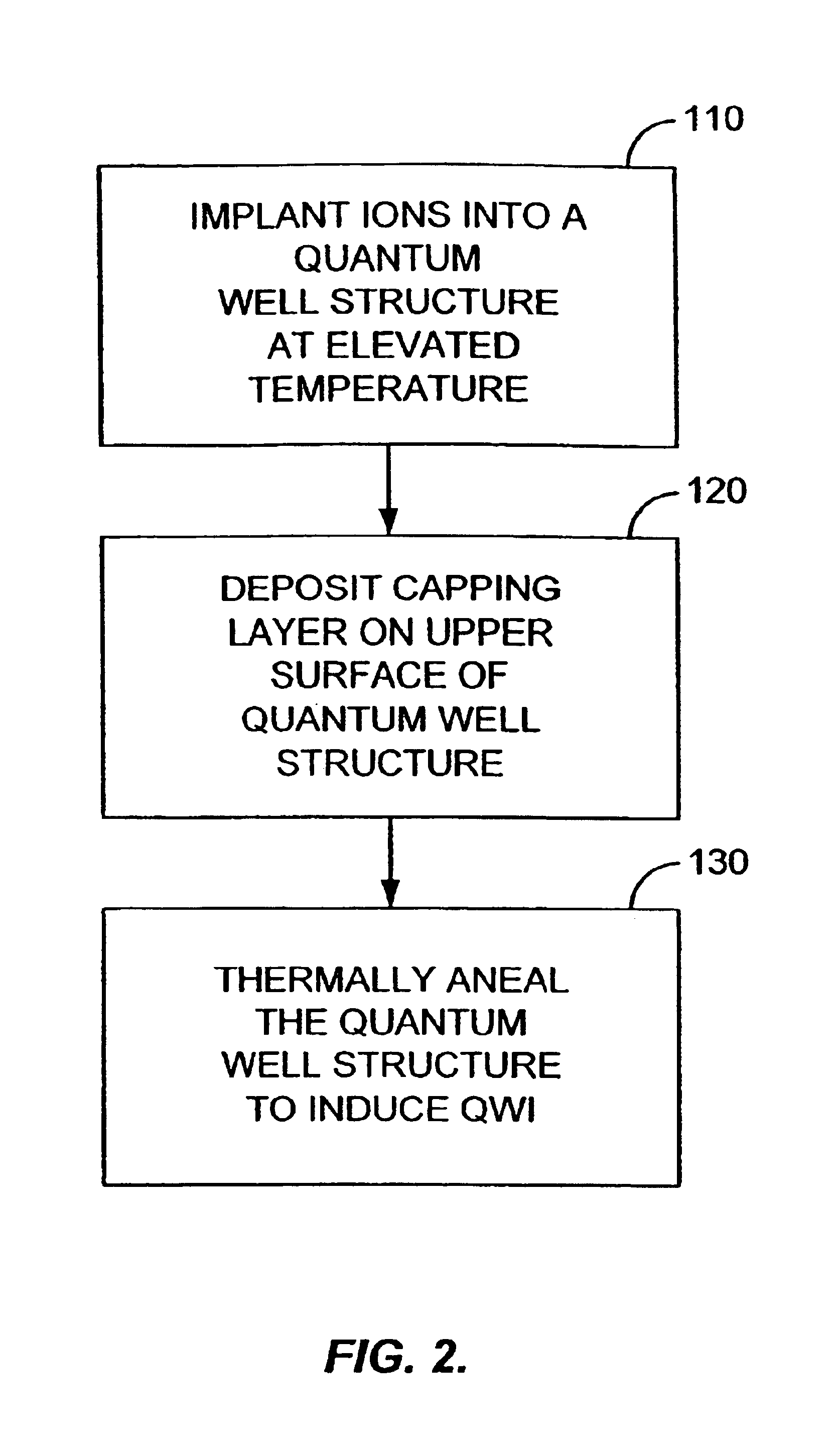
Described herein are various exemplary processes and embodiments of the inventive TAIVID process. The processes can, for example, be used to monolithically integrate various photonic devices on the same substrate (e.g., a wafer), wherein the various photonic devices possess different quantum-well bandgap energies.

To be consistent throughout the present specification and for clear understanding of the present invention, the following definitions are hereby provided for terms used therein:

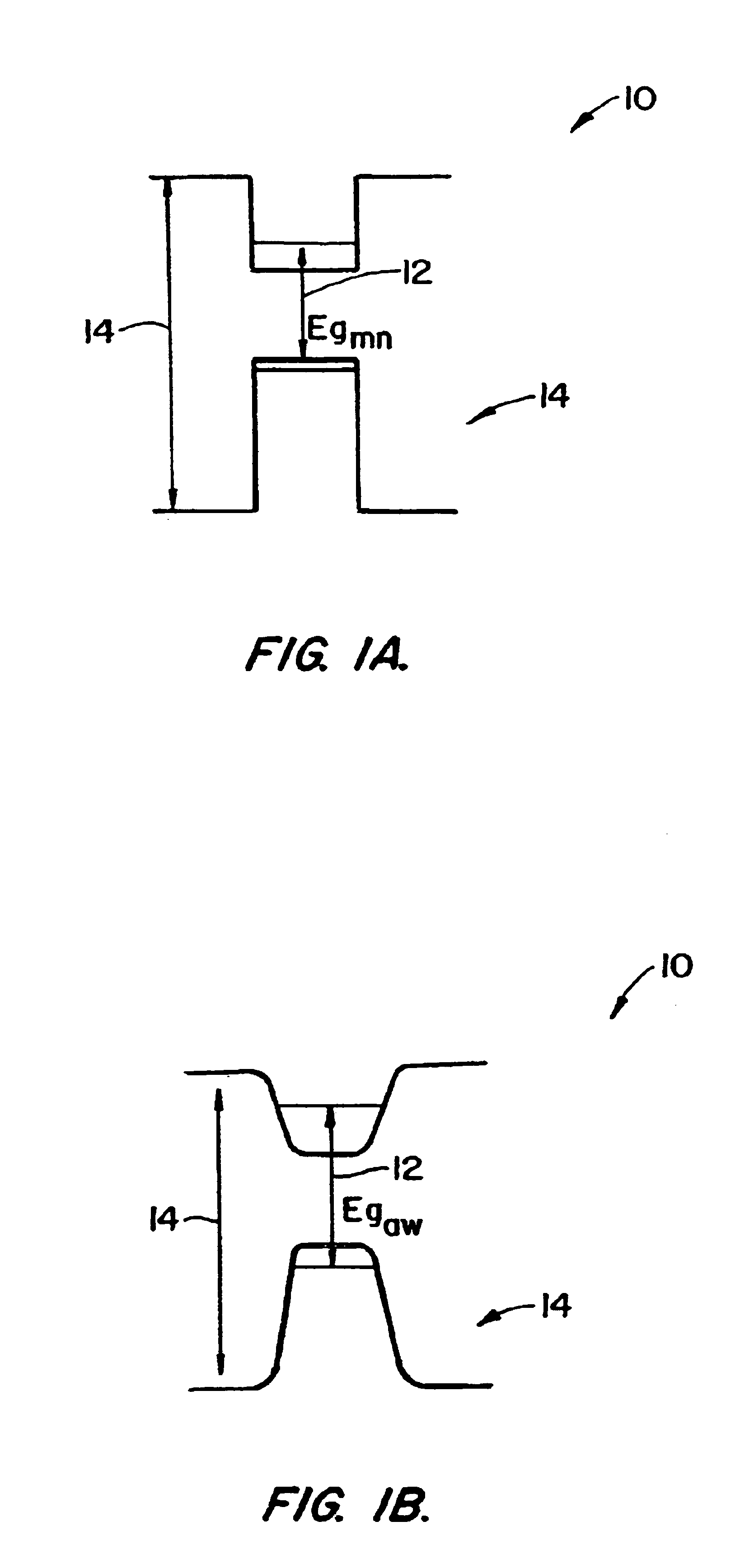
The term “deep-level ion species” refers to atomic species that are not ionized in III-V semiconductor materials at room temperature; and

The term “shallow-level ion species” refers to atomic species that become electrically active at room temperature.

The term “indirect-well implantation” refers to a process which utilizes an implantation condition for which the range of peak impurity and / or vacancy concentration is placed ≧0.5 μm away from a quantum well structure.

The term “direct-well implantation” ...


PUM


Abstract

A process for shifting the bandgap energy of a quantum well layer (e.g., a III-V semiconductor quantum well layer) without inducing complex crystal defects or generating significant free carriers. The process includes introducing ions (e.g., deep-level ion species) into a quantum well structure at an elevated temperature, for example, in the range of from about 200° C. to about 700° C. The quantum well structure that has had ions introduced therein includes an upper barrier layer, a lower barrier layer and a quantum well layer. The quantum well layer is disposed between the upper barrier layer and the lower barrier layer. The quantum well structure is then thermally annealed, thereby inducing quantum well intermixing (QWI) in the quantum well structure and shifting the bandgap energy of the quantum well layer. Also, a photonic device assembly that includes a plurality of operably coupled photonic devices monolithically integrated on a single substrate using the process described above.

Description

BACKGROUND OF THE INVENTION1. Field of the InventionThe present invention relates, in general, to photonic device manufacturing methods and, in particular, to methods for shifting the bandgap energy of quantum well layers and photonic devices and photonic integrated circuits formed thereby.2. Description of the Related ArtIn the manufacturing of photonic devices, it is often desirable to employ processes that facilitate the monolithic integration of multiple photonic devices on a single substrate. This monolithic integration increases the yield, performance and functionality of the photonic devices and reduces manufacturing cost. The multiple photonic devices can include active photonic devices (e.g., lasers, optical intensity modulators, optical phase modulators, optical switches, optical amplifiers, optical saturable absorbers, optical pulse reconditioners, optical wavelength converters, phosistors [photon transistors], variable optical attenuators, optical detectors) and passive ...

Claims


Application Information

Patent Timeline
Patent Type & Authority Patents(United States)
IPC IPC(8): H01L21/18H01L21/02H01S5/34H01S5/026H01S5/00
CPCB82Y20/00H01L21/182H01S5/026H01S5/3414H01S5/0265H01S5/3413H01S5/0261
Inventor OOI, BOON-SIEWHO, SENG-TIONG
Owner HO SENG TIONG
Why Eureka
Try Eureka