Process for producing a multi-layer printer wiring board

Inactive Publication Date: 2005-04-19
AJINOMOTO CO INC
View PDF38 Cites 15 Cited by
  • Summary
  • Abstract
  • Description
  • Claims
  • Application Information

AI Technical Summary

Benefits of technology

[0009]Accordingly, one object of the present invention is to provide an inter-laminar adhesive film that is useful in multi-layer printed wiring boards, among other things, and gives excellent embedding properties in the internal-layer circuit.
[0010]A further object of the present invention is to provide an inter-laminar adhesive film that provides excellent surface smoothness when used in production of multi-layer printed wiring boards.
[0011]A further object of the present invention is to provide a process for production of a multi-layer printed wiring board at high productivity levels usi

Problems solved by technology

However, the process is costly and conducts heating and molding under pressure through lamination pressing, thus requiring large equipment and a long processing time.
Additionally the process requires the use of glass cloth with a relatively high dielectric constant as the prepreg sheet, which limits the ability to reduce the inter-laminar thickness.
The process is also problematic because of the insulation concern due to CAF.
Because the underlining adhesive layer is formed in an ink form by these methods, however, the possibility of dust contamination into the adhesive layer during the processes i

Method used

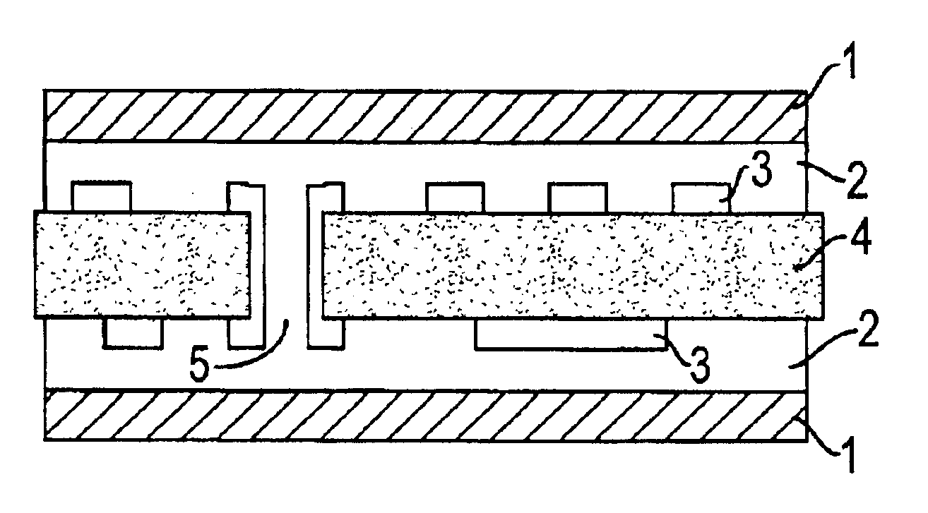
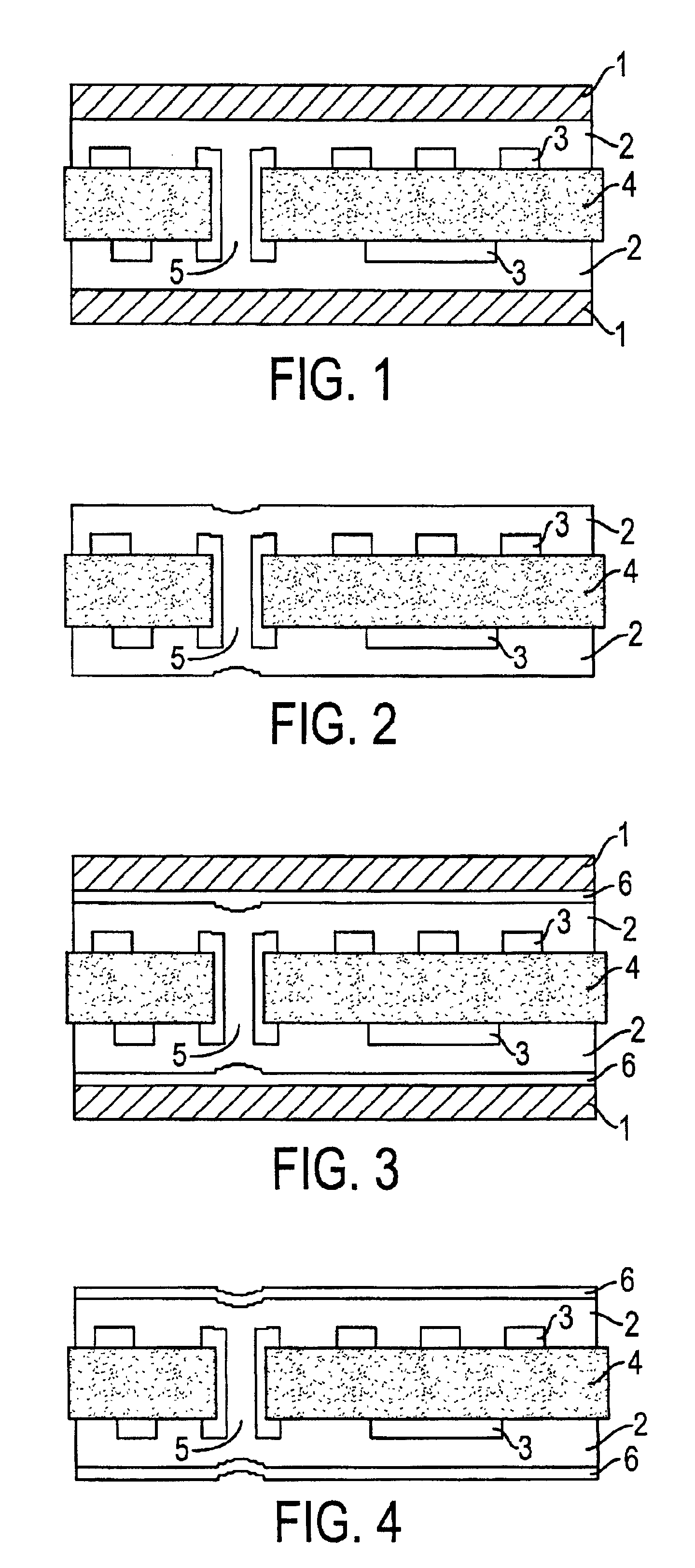

Image

  • Process for producing a multi-layer printer wiring board
  • Process for producing a multi-layer printer wiring board

Examples


example 1

[0057]Thirty parts by weight of a fluid bisphenol A epoxy resin (with an epoxy equivalent of 185, Epicoat 828 EL manufactured by Oil Shell Epoxy, Co., Ltd.) As the component A (the amount to be blended is hereinafter represented in parts by weight), 20 parts by weight of a bisphenol A epoxy resin (with an epoxy equivalent of 2000 and a softening point of 124° C., Epicion 7051 manufactured by Dai-Nippon Ink Chemistry, Co., Ltd.) as the component B, and 40 parts by weight of a brominated bisphenol A epoxy resin (with an epoxy equivalent of 499, a softening point of 75° C. and a bromide content of 21% by weight, YDB-500 manufactured by Toto Chemical Industry, Co., Ltd.) were dissolved in methyl ethyl ketone (abbreviated as MEK hereinafter) under heating and agitation, to which were added epoxy curing agents as the component (C), namely 4 parts by weight of 2,4-diamino-6-(2-methyl-1-imidazolylethyl)-1,3,5-triazine isocyanuric acid adduct, 2 parts by weight of finely ground silica and 4 ...

example 2

[0058]Twenty parts by weight of a fluid bisphenol A epoxy resin (Epicoat 828 EL manufactured by Oil Shell Epoxy, Co., Ltd.) as the component A, 20 parts by weight of a brominated bisphenol A epoxy resin (YDB-500, manufactured by Toto Chemical Industry, Co., Ltd.) And 20 parts by weight of cresol novolak epoxy resin (with an epoxy equivalent of 215 and a softening point of 78° C.; Epiclon N-673, manufactured by Dai-Nippon Ink Chemistry, Co., Ltd) as the component B′, and 15 parts by weight of a polybutadiene rubber with its terminus epoxylated (Denalex R-45EPT, manufactured by Nagase Chemical Industry, Co., Ltd.) were dissolved in MEK under heating and agitation, to which were added 50 parts by weight of a brominated phenoxy resin varnish (at a non-volatile content of 40% by weight and a bromide content of 25% by weight in a solvent composition of xylene: methoxypropanol: methyl ethyl keton=5:2:8, YPB-40-PXM40, manufactured by Toto Chemical Industry, Co., Ltd.) as the component (D), ...

example 3

[0059]The resin composition varnish as described in Example 2 was coated on a PET film of a thickness of 50 μm to a final dried thickness of 100 μm by means of a roller coater, followed by drying at 80 to 120° C. for 13 minutes to prepare an adhesive film (at a content of the residual solvents at 4% by weight). The film was folded at an angle of 180 degrees so as to access the flexibility, and no abnormalities such as cracks were found in the resin part.


PUM

PropertyMeasurementUnit
Temperatureaaaaaaaaaa
Percent by massaaaaaaaaaa

Abstract

The present invention is directed to an inter-laminar adhesive composition containing a liquid epoxy resin, a polyfunctional epoxy resin having a softening point higher than a lamination temperature of the adhesive and with two or more epoxy groups within the molecule; and a latent epoxy curing agent initiating a reaction at a temperature higher than the lamination temperature. The adhesive composition optionally contains a liquid resin other than the liquid epoxy resin and/or an organic solvent and the liquid resin includes the liquid epoxy resin, the organic solvent or both constituting from 10 to 55% by weight of the composition.
This inter-laminar adhesive composition allows for the preparation of a multi-layer printed wiring board. The process for preparing the multi-layer printed wiring board is provided. The resulting multi-layer printed wiring board of the invention possesses excellent embedding properties in the internal-layer circuit, excellent surface smoothness and can be provided at high productivity levels in a building up process using the present adhesive.

Description

CROSS-REFERENCE TO RELATED APPLICATIONS[0001]This is a divisional of U.S. application Ser. No. 09 / 721,664 filed Nov. 27, 2000; which is now U.S. Pat. No. 6,376,053; which is a continuation of U.S. application Ser. No. 08 / 999,332, filed Dec. 29, 1997, now abandoned.BACKGROUND OF THE INVENTION[0002]1. Field of the Invention[0003]The present invention relates to an inter-laminar film adhesive for multi-layer printed wiring boards, capable of integrally carrying out the coating process of an inner-layer circuit pattern and the filling process of a resin in a superficial via hole and / or a through-hole simultaneously on a multi-layer printed wiring board of a build-up type where a conductive layer and an insulation layer are alternatively built up; and a process for producing a multilayer printed wiring board using the same.[0004]2. Discussion of the Background[0005]Conventional processes for producing a multi-layer printed wiring board generally comprise lamination pressing through sever...

Claims


Application Information

Patent Timeline
IPC IPC(8): C08L63/00H05K3/46H05K1/00
CPCC08L63/00H05K3/4655H05K3/4661H05K3/4652H05K3/4676H05K2201/0209Y10T428/24917H05K2201/0355H05K2203/066H05K2203/0773Y10S428/901Y10T428/287H05K2201/0212H05K3/00
Inventor NAKAMURA, SHIGEOYOKOTA, TADAHIKO
Owner AJINOMOTO CO INC
Why Eureka
Try Eureka