Strained-channel transistor and methods of manufacture

a strain-channel transistor and manufacturing method technology, applied in the direction of transistors, semiconductor devices, electrical apparatus, etc., can solve the problems of high defect density of substrates, high approach cost, and strain relaxation, and achieve the effect of improving the performance of both n-channel and p-channel transistors

Inactive Publication Date: 2005-04-19
TAIWAN SEMICON MFG CO LTD
View PDF42 Cites 116 Cited by
  • Summary
  • Abstract
  • Description
  • Claims
  • Application Information

AI Technical Summary

Benefits of technology

[0012]Aspects of this invention address the drawbacks of the prior art by optimizing the isolation structure induced strain for n-channel and p-channel transistors separately. For example, n-channel and p-channel transistors are each provided with strained channel regions. In particular, embodiments of the invention teach a structure and method of engineering the strain in the channel of the transistor by engineering the isolation structure to improve the performance of both the n-channel and p-channel transistors.

Problems solved by technology

But there are concerns about the strain relaxation upon subsequent CMOS processing where high temperatures are used.
In addition, this approach is very expensive since a SiGe buffer layer with thickness in the order of micrometers has to be grown.
Numerous dislocations in the relaxed SiGe buffer layer exist and some of these dislocations propagate to the strained silicon layer, resulting in a substrate with high defect density.
Thus, this approach has limitations that are related to cost and fundamental material properties.
However, uniaxial tensile strain degrades the hole mobility while uniaxial compressive strain degrades the electron mobility.
Ion implantation of germanium can be used to selectively relax the strain so that the hole or electron mobility is not degraded, but this is difficult to implement due to the close proximity of the n and p-channel transistors.
While there is much prior art related to the formation and improvement of the isolation structure, e.g., U.S. Pat. No. 6,046,487, U.S. Pat. No. 5,763,315, and U.S. Pat. No. 5,447,884, this prior art has not addressed the separate optimization of strain for the n-channel and p-channel transistors.

Method used


Image

  • Strained-channel transistor and methods of manufacture
  • Strained-channel transistor and methods of manufacture
  • Strained-channel transistor and methods of manufacture

Examples


first embodiment

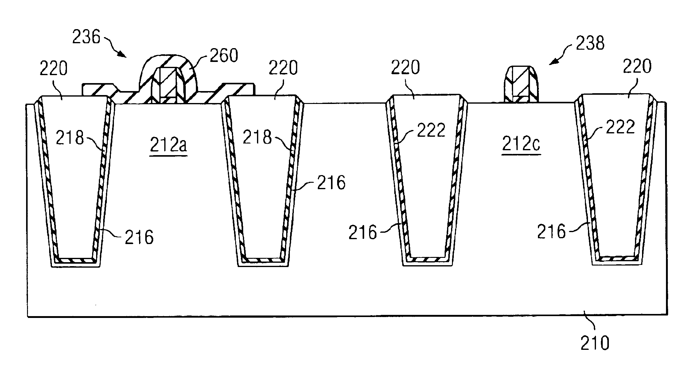
[0037]As shown in FIGS. 4a and 4b, a second isolation structure 214c / d is employed to define a second active region 212c, which will be provided with in-plane compressive strain. In a first embodiment, as shown in FIG. 4a, the second isolation structure 214c / d is a trench isolation structure with a silicon oxide liner 216 underlying an ion-implanted silicon nitride liner 222. The ion implantation introduces defects into the silicon nitride liner film 222 and causes it to lose or degrades its ability to block oxygen diffusion. Therefore, it is possible for oxygen to diffuse through silicon nitride 222 and result in further oxidation of the trench sidewall, causing volume expansion in a confined space, and therefore introducing in-plane compressive stress in the second active region.

[0038]The in-plane compressive stress results in an in-plane compressive strain in the crystal lattice of the material comprising the second active region 212c. It is desired that this in-plane compressive...

second embodiment

[0039]In a second embodiment, as shown in FIG. 4b, the second isolation structure 214c / d is a conventional trench isolation structure with a silicon oxide liner (not shown) and with no silicon nitride liner. The second isolation structure resembles the isolation structure of FIG. 3a and therefore results in an in-plane compressive strain in the second active region.

[0040]According to the preferred embodiment of the present invention, the first and second active regions 212a and 212c are provided on the same semiconductor substrate 210. By having the flexibility of providing active regions with different strain conditions, it is therefore possible to optimize the performance of n-channel and p-channel transistors by the choice and use of the appropriate strain conditions in the active regions. For example, n-channel transistors (not shown in FIG. 4) may be formed on the first active region 212a with tensile strain in their source-to-drain direction to improve their drive current perf...

third embodiment

[0068]In the third embodiment method, another process flow is provided for forming active regions with different strain conditions. The starting material is a semiconductor substrate as shown in FIG. 8a. Trenches 232 are formed in the semiconductor substrate 210 using a first mask 230, as shown in FIG. 8b. A liner oxide 216, such as thermally grown silicon oxide, is then formed on at least the sidewalls of the trenches, as shown in FIG. 8c. It is understood that the liner oxide may also be formed by deposition techniques.

[0069]A second patterned mask 235 is formed to cover the second active region 212c, while exposing the first active region 212a, as shown in FIG. 8d. The mask 235 may cover all or a portion of the trenches 232. Liner oxide 216 not covered by the second patterned mask may be nitrided. The nitridation process forms a nitrided liner 217 and may include an ion implantation of nitrogen containing species, an anneal in a nitrogen-containing ambient, or exposure to nitroge...


PUM


Abstract

A semiconductor device includes a region of semiconductor material with first and second isolation trenches formed therein. The first isolation trench is lined with a first material having a low oxygen diffusion rate and is filled with an insulating material. The second isolation trench is not lined with the first material but is filled with an insulating material. A first transistor is formed adjacent the first isolation region and a second transistor formed adjacent the second isolation region.

Description

TECHNICAL FIELD[0001]The present invention relates generally to semiconductor devices and more particularly to a strained channel transistor and methods of manufacturing the same.BACKGROUND[0002]Size reduction of metal-oxide-semiconductor field-effect transistors (MOSFET), including reduction of the gate length and gate oxide thickness, has enabled the continued improvement in speed performance, density, and cost per unit function of integrated circuits over the past few decades.[0003]To enhance transistor performance further, strain may be introduced in the transistor channel for improving carrier mobilities. Therefore, strain-induced mobility enhancement is another way to improve transistor performance in addition to device scaling. There are several existing approaches of introducing strain in the transistor channel region.[0004]In one conventional approach, as described in a paper by J. Welser et al., published at the December 1992 International Electron Devices Meeting held in ...

Claims


Application Information

Patent Timeline
Patent Type & Authority Patents(United States)
IPC IPC(8): H01L21/762H01L21/70H01L27/12H01L21/8238
CPCH01L21/76229H01L21/76237H01L21/76283H01L29/7842H01L21/823878H01L27/1203H01L21/823807H01L29/7846
Inventor YEO, YEE-CHIAKO, CHIH-HSINLEE, WEN-CHINHU, CHENMING
Owner TAIWAN SEMICON MFG CO LTD
Why Eureka
Try Eureka