Chamber effluent monitoring system and semiconductor processing system comprising absorption spectroscopy measurement system, and methods of use
a technology of absorption spectroscopy and monitoring system, which is applied in the direction of optical radiation measurement, semiconductor/solid-state device testing/measurement, instruments, etc., can solve the problems of reducing product yield, molecular impurities such as moisture, and water vapor is especially detrimental to the devices fabricated in the processing tools
- Summary
- Abstract
- Description
- Claims
- Application Information
AI Technical Summary
Benefits of technology
Problems solved by technology
Method used
Image


Examples
example 1
[0064]As described below, moisture concentration in a semiconductor processing system during etching is monitored, using the operating procedure described below.
[0065]As the semiconductor processing system, an Applied Materials Precision 5000 plasma etching system is used in conjunction with a TDLAS measurement system. The measurement system is set up for water vapor measurement to determine the drydown characteristics of the processing chamber.
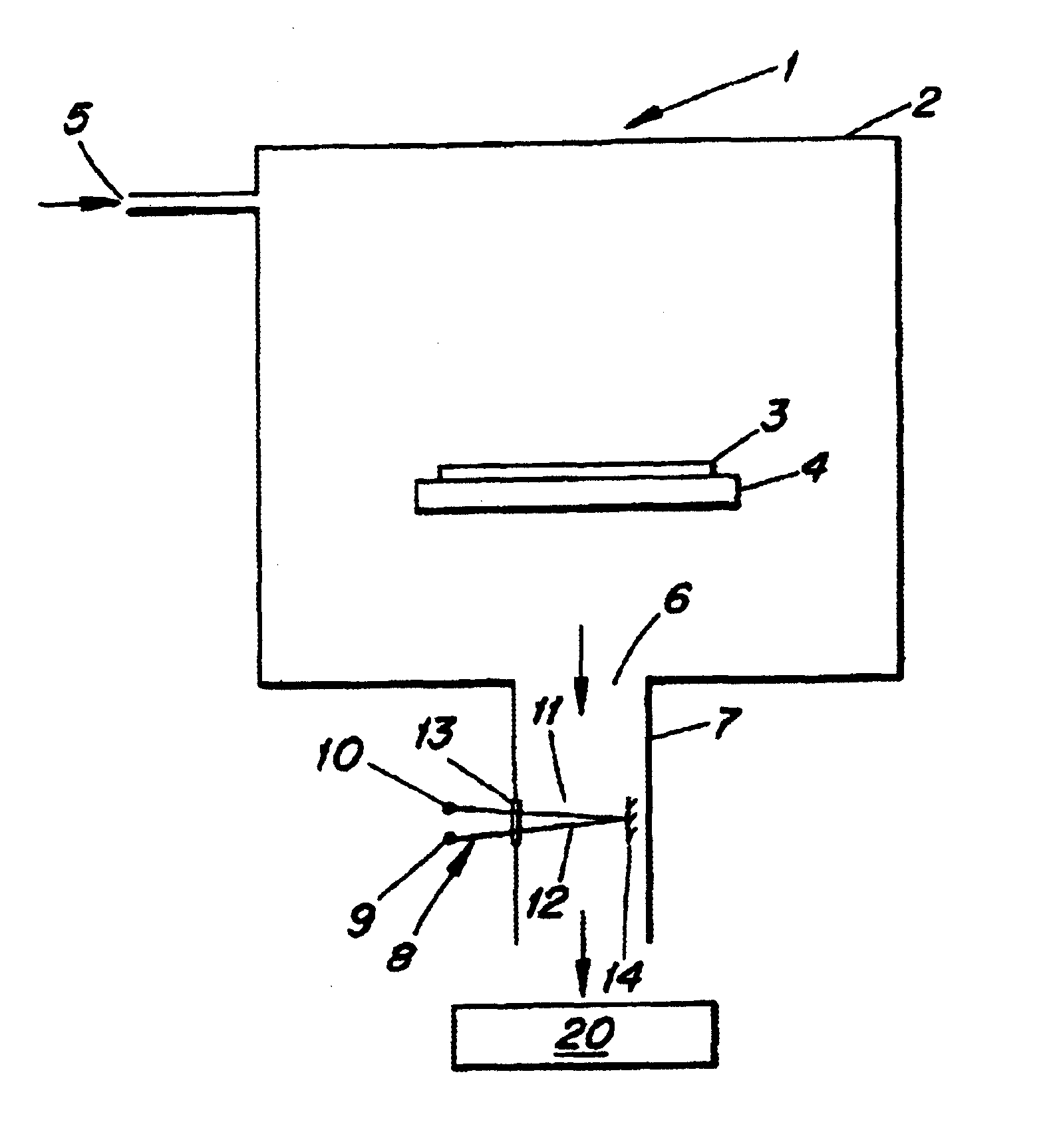
[0066]The measurement system sample region is disposed in the exhaust line of the etching tool. The light transmissive inlet and outlet windows are disposed directly across from each other in the walls of the exhaust line, with the sample region disposed therebetween, such that the light emitted by the laser diode passes straight through the inlet window to the outlet window.
[0067]The diode is manufactured by Sensors Unlimited Inc., and is composed of InGaAsP / InP. The diode is fabricated in order to emit light in the wavelength region includi...
example 2
[0073]Using the same etching tool described above in reference to Example 1, CO is monitored in a plasma ASH process wherein photoresist from an etched substrate is stripped. In the measurement system, a Pb-salt diode manufactured by Laser Photonics Corp. is mounted in a Laser Analytics liquid nitrogen-cooled coldhead. A one inch diameter, aspheric, antireflective coated, F / 1 ZnSe lens is used to collimate the beam. The detector is a Graseby HgCdTe Model 1710112, with a 10-MHz bandwidth amplifier. Laser current is controlled by an ILX Lightwave LDX-3620, and the temperature is controlled by a Lake Shore DRC-910A controller. The wavelength of the light emitted by the laser diode is locked to the characteristic value for CO, i.e., 4.7 μm, using a feedback signal to the laser diode. A signal corresponding to the third derivative of the absorption signal is used.
[0074]After loading the semiconductor substrate into the etching chamber, O2 at a flow rate of 60 sccm is introduced into the ...
PUM
 Abstract
Description
Claims
Application Information