Thin film device

a thin film, thin film technology, applied in the direction of semiconductor devices, basic electric elements, electrical equipment, etc., can solve the problems of difficult epitaxial thin film formation, high cost of sapphire substrate and sic substrate, and difficult direct epitaxial growth of ionic bond thin film on sic substrate, etc., to achieve easy deposited, improve characteristics, and reduce costs

Inactive Publication Date: 2005-05-03
NAT INST FOR MATERIALS SCI
View PDF5 Cites 13 Cited by
  • Summary
  • Abstract
  • Description
  • Claims
  • Application Information

AI Technical Summary

Benefits of technology

[0035]As described above, according to the invention, the ZnS buffer layer deposited on the Si substrate by epitaxial growth or the buffer layer having the ZnO / ZnS, STO / ZnS, and Pt / ZnS structures is interposed, whereby the thin film device where the ionic crystals are epitaxially grown on the Si substrate is easily deposited, expecting improvements in characteristics. Particularly, when GaN is formed as the ionic crystal, a thin film device using GaN can be fabricated at lower costs than traditional fabrication methods.
[0036]In addition, the buffer layer of the ZnO / ZnS, STO / ZnS, and Pt / ZnS structures is used, instead of using the single ZnS buffer layer, whereby evaporation of Zn, S or ZnS from the surface of the ZnS layer can be suppressed, thus serving to prevent the impurity contamination of these in the subsequent deposition of ionic crystals and also prevent contamination over a thin film fabricating apparatus.

Problems solved by technology

However, it is hard to form the epitaxial thin film of these, having been conducting various attempts.
However, the sapphire substrate and the SiC substrate are expensive, thus preferably forming it on a Si substrate.
In the mean time, it is hard to directly epitaxially grow an ionic bond thin film on the Si substrate.
The lattice defects cause the mobility of carriers to be dropped, or cause the luminous efficiency of a luminescent layer or the lifetime of a thin film device to be deteriorated.
However, it is inevitable to oxidize the Si surface, and there is a problem that the film quality of a buffer layer formed on SiO2 is not so excellent.
In addition, there is a problem that a buffer layer using TiN or TaN is not excellent as well because of generating SiNx.

Method used


Image

  • Thin film device
  • Thin film device
  • Thin film device

Examples


embodiment 1

[0060][Embodiment 1]

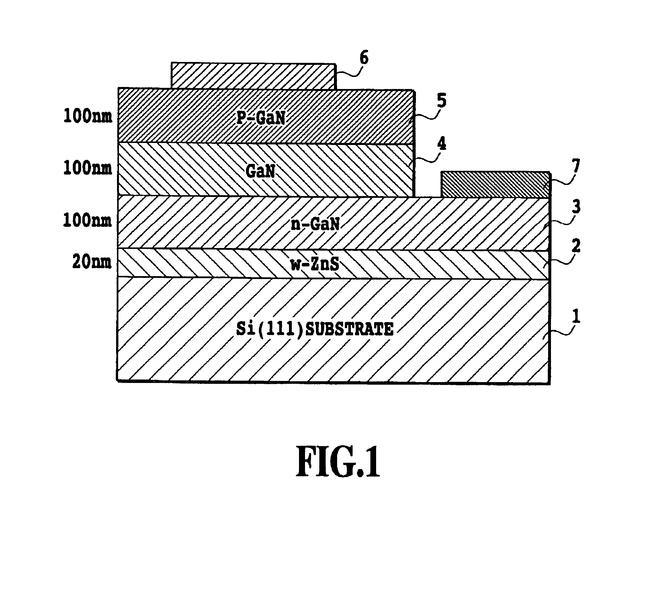
[0061]FIG. 1 shows a diagram illustrating a configuration of a GaN light emitting diode device formed according to the invention. In the drawing, 1 denotes a Si (111) single crystal substrate, 2 denotes a W-ZnS layer (20 nm; W indicates zinc sulfide of the wurtzite structure) deposited on the single crystal substrate 1, 3 denotes an n-GaN layer 3 (100 nm) deposited on the W-ZnS layer 2, 4 denotes a GaN layer (100 nm) deposited on the n-GaN layer, which functions as a luminescent layer, 5 denotes a p-GaN layer (100 nm) deposited on the GaN layer 4, 6 denotes an upper electrode formed on the p-GaN layer 5, and 7 denotes a lower electrode formed on the n-GaN layer 3.

[0062]The Si (111) single crystal substrate was removed of a natural oxide film with Hydrogen Fluoride, cleaned with water, and then placed in a deposition chamber for vacuuming for about ten minutes. ZnS was deposited about 20 nm in thickness at a substrate temperature of 750° C. by Pulsed Laser Deposit...

embodiment 2

[0092][Embodiment 2]

[0093]FIG. 10 shows a diagram illustrating a configuration of a thin film capacitor device fabricated according to the invention. In the drawing, 11 denotes an n-type Si (111) substrate, 12 denotes an Al doped W-ZnS layer (15 nm) deposited on the Si (111) substrate 11, 13 denotes an Al doped W-ZnO layer (400 nm) deposited on the Al doped W-ZnS layer 12, 14 denotes a SrTiO3 layer (190 nm) deposited on the Al doped W-ZnO layer 13, and 15 denotes an upper electrode (200 nm) formed on the SrTiO3 layer 14.

[0094]More specifically, the n-type Si (111) substrate 11 was used to deposit the wurtzite structural ZnS layer 12 of 15 nm in thickness, and the ZnO layer 13 was deposited 400 nm in thickness thereon. Subsequently, the SrTiO3 dielectric layer 14 was deposited, and the Pt upper electrode 15 was formed. A lower electrode is to be the Si substrate 11.

[0095]When ionic crystals such as SrTiO3 or the other perovskite oxides having a lattice constant close to that of plati...

embodiment 3

[0101][Embodiment 3]

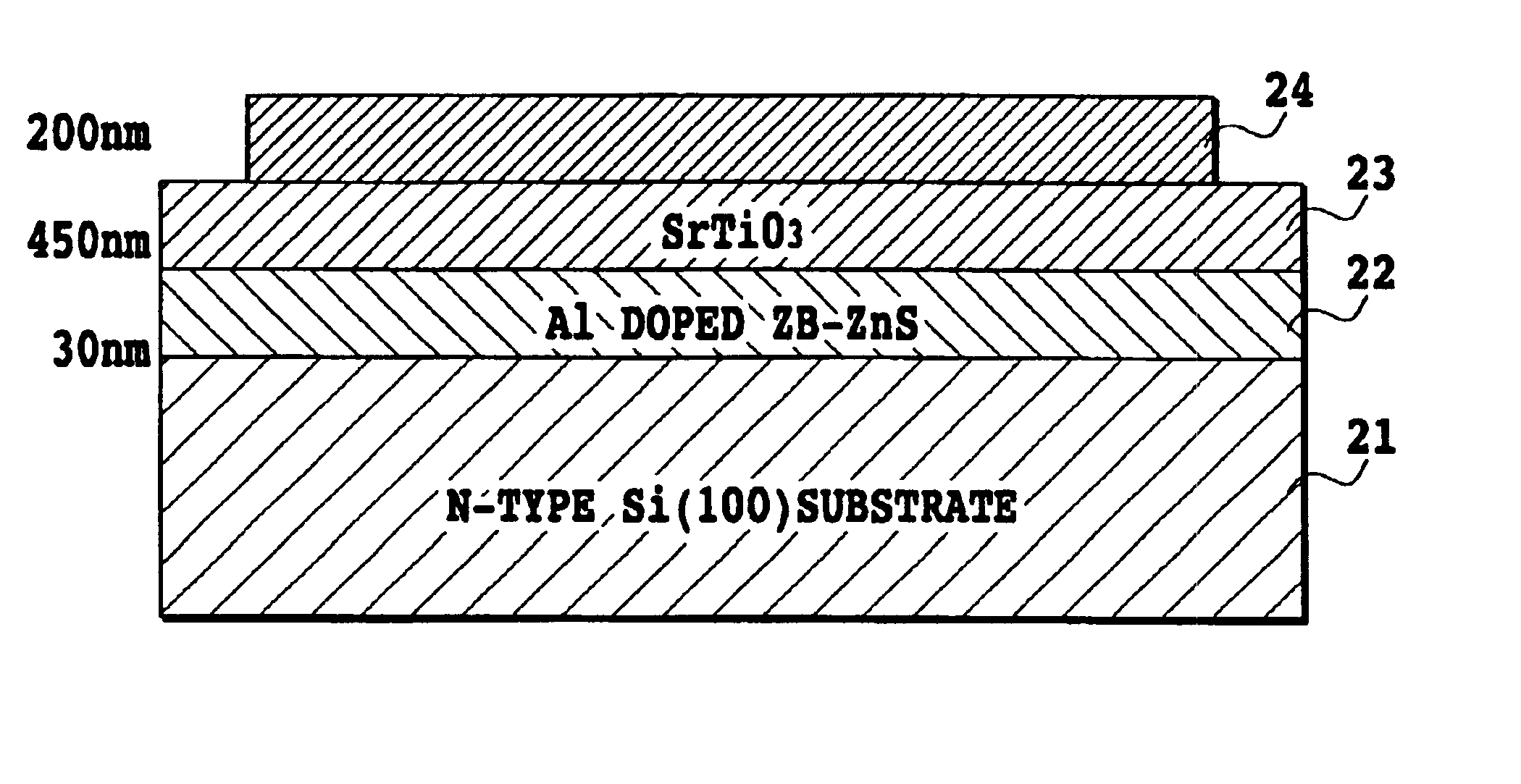
[0102]FIG. 14 shows a diagram illustrating a configuration of a thin film capacitor device fabricated according to the invention. In the drawing, 21 denotes an n-type Si (100) substrate, 22 denotes an Al doped ZB-ZnS layer (40 nm) deposited on the n-type Si (100) substrate 21, 23 denotes a SrTiO3 layer (450 nm) deposited on the Al doped ZB-ZnS layer 22, and 24 denotes an upper electrode (200 nm) formed on the SrTiO3 layer 23.

[0103]More specifically, the n-type Si (100) single crystal substrate 21 was used to deposit the zinc blend structural ZnS layer 22 of 30 nm in thickness, the SrTiO3 dielectric layer 23 was deposited thereon, and subsequently the Pt upper electrode 24 was formed. A lower electrode is to be the Si substrate 21.

[0104]The thin film capacitor device having such the structure is fabricated as follows. First, the n-type Si (100) single crystal substrate with low resistance was removed of a natural oxide film with Hydrogen Fluoride, cleaned with wat...


PUM


Abstract

The invention provides a thin film device where ionic crystals are epitaxially grown on a Si single crystal substrate through a proper buffer layer, and its for fabrication method. A ZnS layer is first deposited on a Si single crystal substrate. Ionic crystal thin films (an n-GaN layer, a GaN layer, and a p-GaN layer) are deposited thereon. The ZnS thin film is an oriented film excellent in crystallinity and has excellent surface flatness. When ZnS can be once epitaxially grown on the Si single crystal substrate, the ionic crystal thin films can be easily epitaxially grown subsequently. Therefore, ZnS is formed to be a buffer layer, whereby even ionic crystals having differences in lattice constants from Si can be easily epitaxially grown in an epitaxial thin film with few lattice defects on the Si single crystal substrate. The characteristics of a thin film device utilizing it can be enhanced.

Description

[0001]This application is based on Japanese Patent Application Nos. 2001-200000 filed Jun. 29, 2001 and 2002-87198 filed Mar. 26, 2002, the contents of which are incorporated hereinto by reference.BACKGROUND OF THE INVENTION[0002]1. Field of the Invention[0003]The present invention relates to a thin film device comprising a compound having ionic bonds (hereafter, it is also called ionic crystals) and its fabrication method, more specifically, to a high intensity light emitting device utilizing an ionic crystal thin film as a functional film (semiconductor laser), a metal insulator semiconductor field effect transistor (MISFET), a high-electron-mobility transistor (HEMT), a thin film capacitor, and the other electronic devices and thin film devices, and fabrication methods.DESCRIPTION OF THE RELATED ART[0004]Many devices using a nitride thin film have been proposed and realized, such as a high intensity light emitting device using a GaN thin film, a MISFET using an AlN / GaN thin film,...

Claims


Application Information

Patent Timeline
Patent Type & Authority Patents(United States)
IPC IPC(8): H01L21/02H01L21/36H01L21/20
CPCH01L21/02381H01L21/02472H01L21/0254H01L21/02491H01L21/02474
Inventor CHIKYOW, TOYOHIROKOINUMA, HIDEOMIKAWASAKI, MASASHIZO, YOO YOUNGKONISHI, YOSHINORIYONEZAWA, YOSHIYUKI
Owner NAT INST FOR MATERIALS SCI
Why Eureka
Try Eureka