

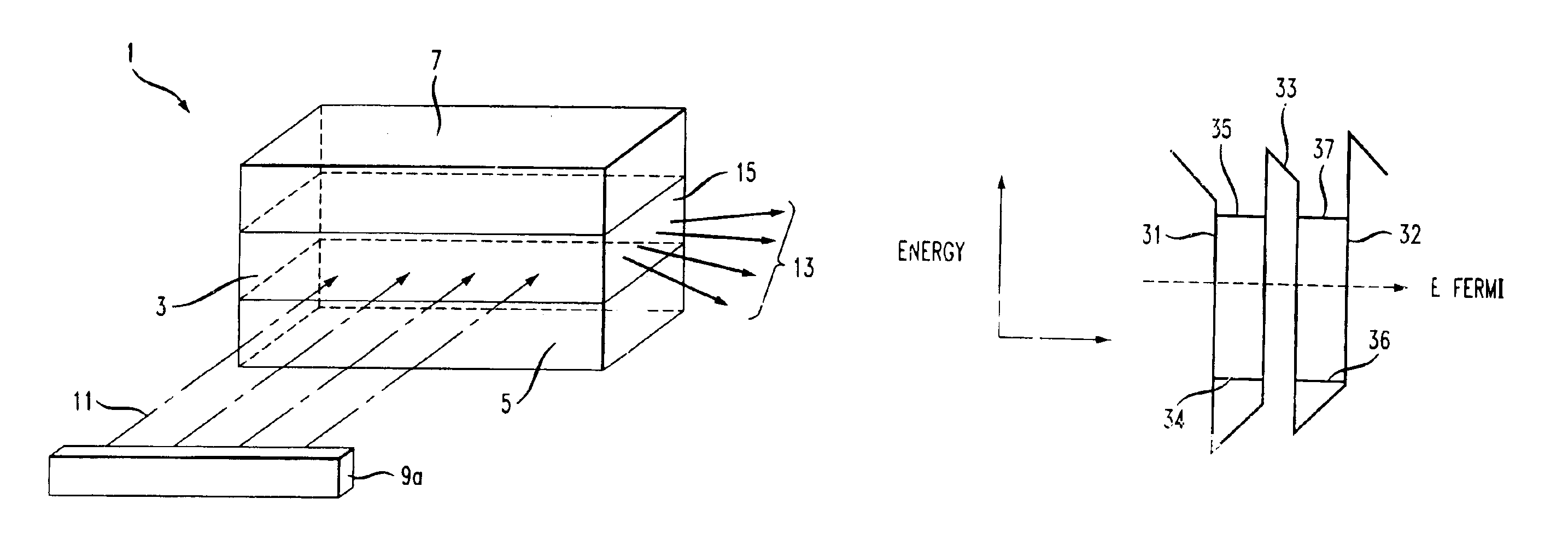
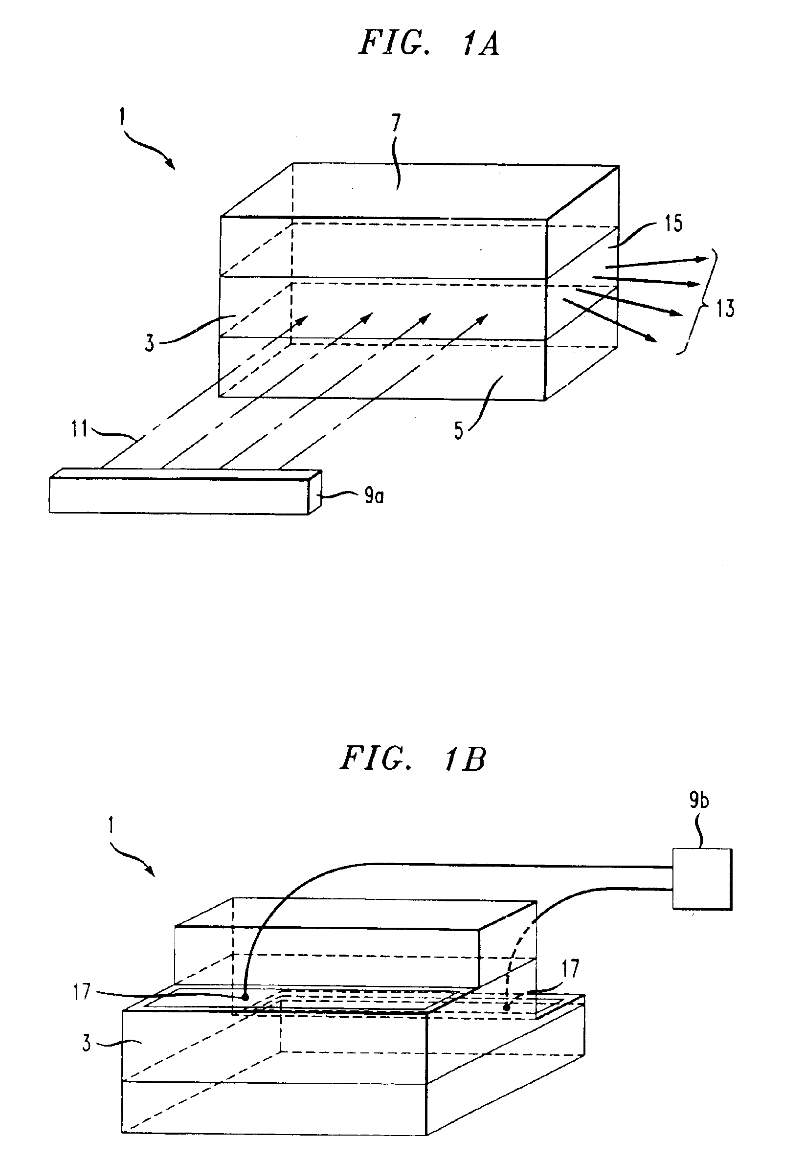
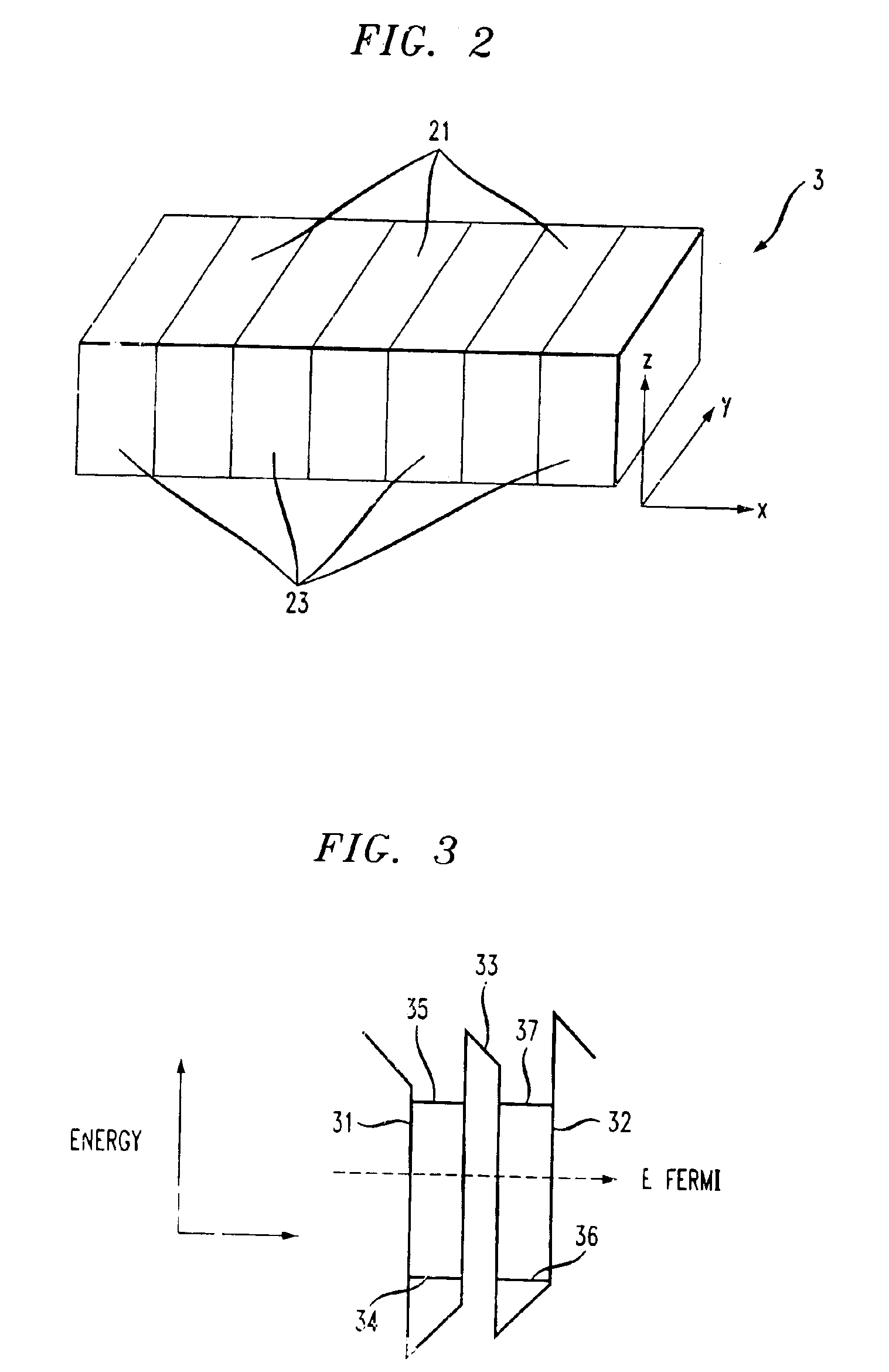
Optical devices with heavily doped multiple quantum wells
a technology of optical devices and quantum wells, applied in the field of optical devices with heavily doped multiple quantum wells, can solve the problems of more complex devices, difficult to determine the exact strength of such fields in large aln-mole fraction materials used for barrier layers, and inability to accurately determine the exact strength of such fields
- Summary
- Abstract
- Description
- Claims
- Application Information
AI Technical Summary
Benefits of technology
Problems solved by technology
Method used
Image

Examples
example 1
[0042]Symmetric and asymmetric coupled DQWs were grown by conventional means. Multi-pass IS-absorption at room temperature was used to probe the energy levels of the quantum well layers. Degenerate doping was employed to establish a common reference energy level. The resulting data show evidence of energy level splitting or “anti-crossing” in symmetric DQWs.
[0043]Table 1 gives an overview of the samples used in these examples. The table provides the sample numbers, referred to hereafter, the nominal layer thicknesses, and AlN-mole fractions. The AlN mole fraction indicates the percentage of aluminum in the quantum well layer. The crystal is grown with 1 atom of metal, i.e., either Al or Ga, per 1 atom of N. Thus, if the AlN mole fraction x equal 0.9, this means that 90% of the atoms are Al and the other 10% of the atoms are Ga. Preferred AlN mole fractions in both the barrier layer, i.e., “dB,” and the barrier region, i.e., “barrier,” are from about 0.5 to 1.0.
[0044]The nominal widt...
example 2
[0047]The structures were modeled by iteratively solving Schroedinger's and Poisson's equations. FIG. 7A and the inset in FIG. 6 show the results of such calculations. An intrinsic electric field in the barrier layers and wells of ±5 MV / cm, respectively, was assumed. It has been verified that the result will be qualitatively the same and quantitatively within a few percent even if zero electric field was assumed.
[0048]It has been established that very narrow quantum well layers, e.g., less than 20 Å wide, are needed to reach IS transitions with wavelengths around 1.55 μm. For coupled quantum well layers 15 Å and 20 Å thick, ground-state anti-crossing energies of 5, 19, 43, and 131 meV for barrier thicknesses of 15, 10, 7, and 3 Å, respectively, were calculated. In particular, a typical barrier thickness where the anti-crossing energy equals the LO phonon energy would be 4.5 Å, i.e., approximately 1.5 monolayers. This may be prohibitively thin taking into account ubiquitous monolayer...
example 3
[0057]So far, only the peak transition energy data have been discussed. However, the full width at half maximum (FWHM) of the observed absorption features also provides valuable information. FIG. 9 displays the FWHM in meV as a function of the peak transition energy in meV for the various samples. The data are grouped by sample type and AlN-mole fraction.
[0058]The numerical values have been extracted from the least square fits as shown in FIGS. 6-8. Gray circles indicate the asymmetric DQWs of FIG. 7B having approximately 0.65 AlN-mole fraction barrier layers. Transitions into the lower-lying state “3” are grouped by a long-dashed ellipsoid. Transitions into the higher-lying level “4” are grouped by the dotted ellipsoid. Solid squares denote the asymmetric DQWs of FIG. 8, and the solid triangles indicate the symmetric DQW of FIG. 6 (N306). The latter three employ approximately 0.90 AlN-mole fraction barrier layers. A plot of the FWHM value as a percentage of the peak transition ener...
PUM
 Abstract
Description
Claims
Application Information