

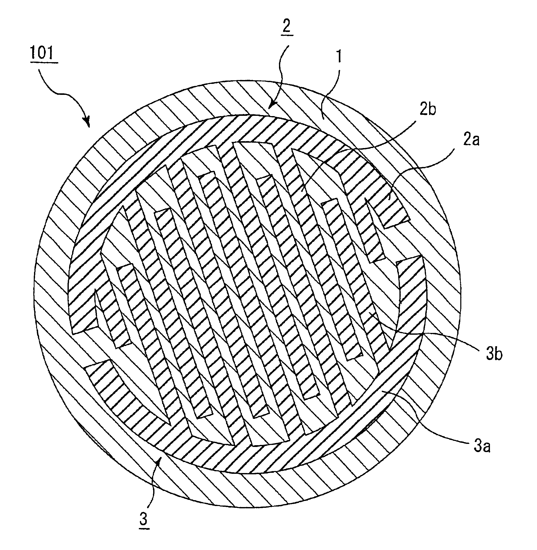
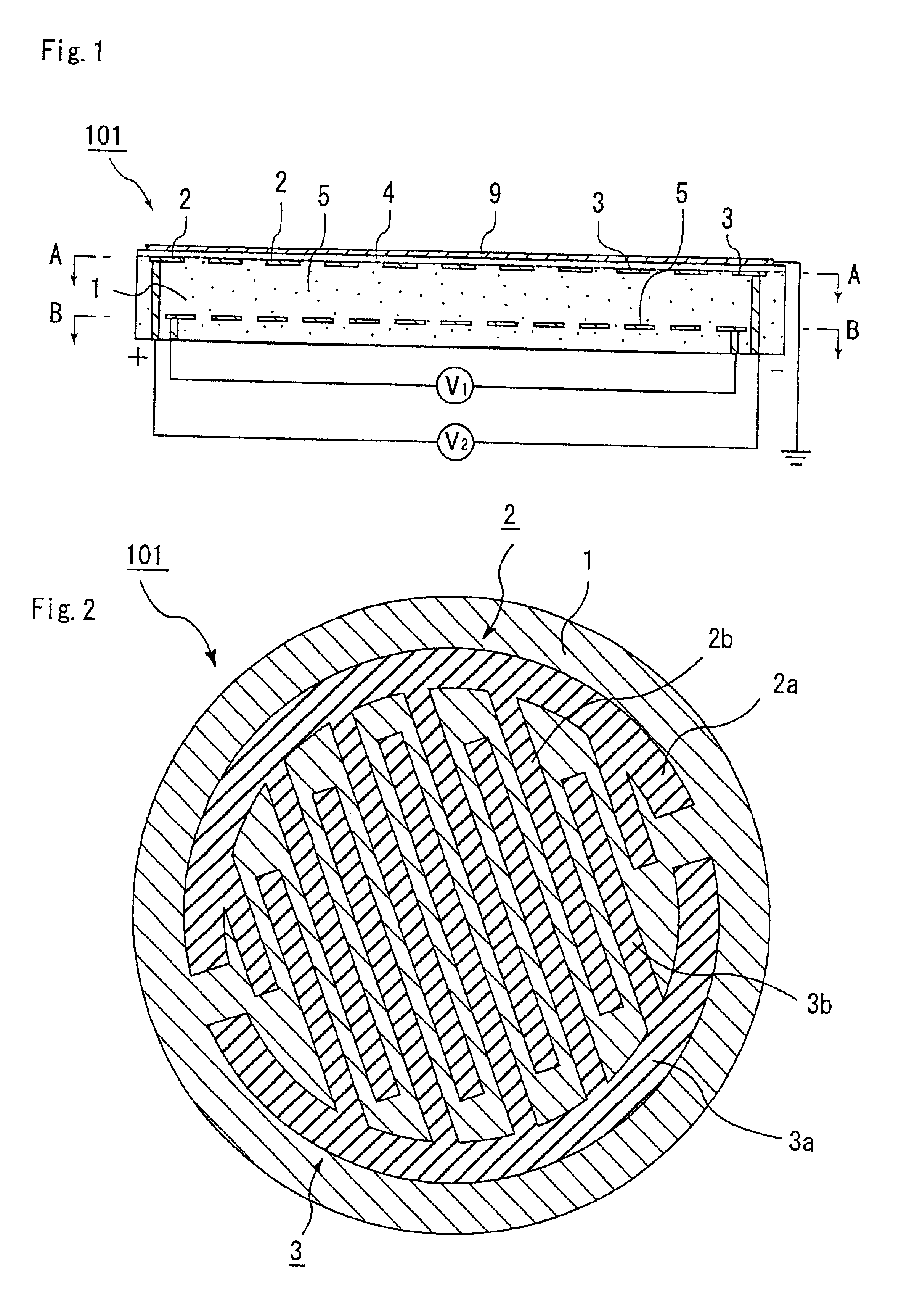
Ceramic substrate for a semiconductor production/inspection device
a ceramic substrate and semiconductor technology, applied in the direction of ohmic-resistance heating, hot plate heating arrangements, coatings, etc., can solve the problem that the breakdown voltage of ceramic dielectric films cannot be easily kept at a high level, and achieve the effect of high temperature and sufficient breakdown voltag
- Summary
- Abstract
- Description
- Claims
- Application Information
AI Technical Summary
Benefits of technology
Problems solved by technology
Method used
Image

Examples
example 4
Production of an Electrostatic Chuck 401 (Reference to FIG. 6)
[0256]The steps (1) to (5) (with the condition in the first line in Table 3) in Example 2 were carried out and then nickel was thermally sprayed onto the bottom surface. Thereafter, a lead / tellurium type Peltier device was jointed thereto, so as to obtain an electrostatic chuck 401.
[0257]The thus-produced electrostatic chuck was superior in temperature-falling property. Thus, when the chuck was cooled by means of the Peltier device, the temperature fell from 450 ° C. to 100° C. in 3 minutes.
example 5
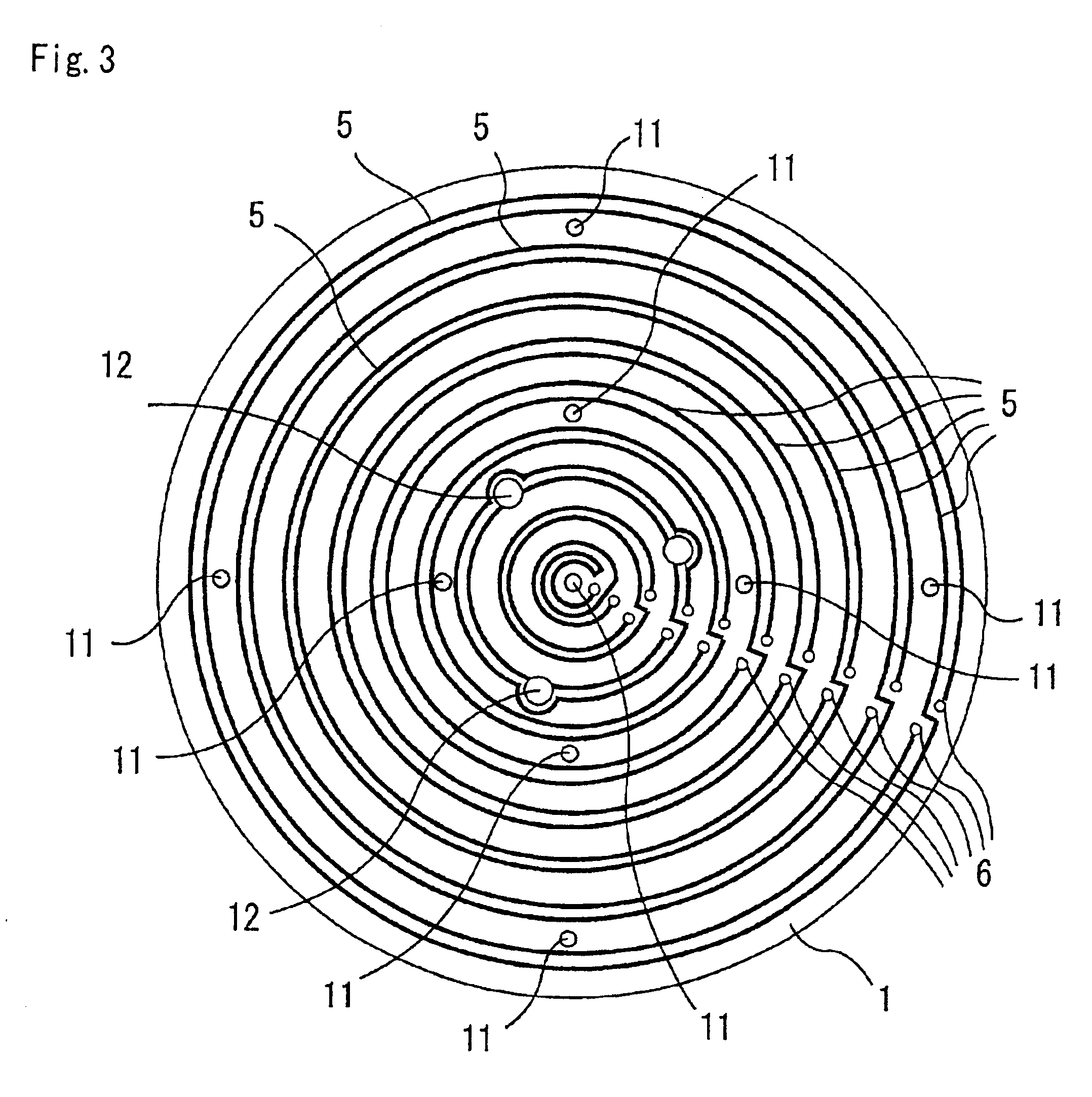
Production of a Wafer Prober 601 (Reference to FIG. 11)
[0258](1) The following paste was used to conduct formation by a doctor blade method to obtain a green sheet of 0.47 mm in thickness: a paste obtained by mixing 1000 parts by weight of aluminum nitride powder (made by Tokuyama Corp., average particle diameter: 1.1 μm) fired at 500° C. for 1 hour in the air, 40 parts by weight of yttria (average particle diameter: 0.4 μm), 10 parts by weight of SiC and 530 parts by weight of mixed alcohols of 1-butanol and ethanol.[0259](2) Next, this green sheet was dried at 80° C. for 5 hours, and subsequently through holes for conductor-filled through holes for connecting external terminals pins to heating elements were made by punching.[0260](3) The following were mixed to prepare a conductor containing paste A: 100 parts by weight of tungsten carbide particles having an average particle diameter of 1 μm, 3.0 parts by weight of an acrylic binder, 3.5 parts by weight of α-terpineol solvent, an...
PUM
| Property | Measurement | Unit |
|---|---|---|
| pore diameter | aaaaa | aaaaa |
| porosity | aaaaa | aaaaa |
| diameter | aaaaa | aaaaa |
Abstract
Description
Claims
Application Information