Highly compact non-volatile memory and method therefor with internal serial buses

a non-volatile memory, high-compact technology, applied in static storage, digital storage, instruments, etc., can solve the problems of unsuitable large disk drive volume, and inability to meet the needs of mobile and handheld environment, and achieve significant space and power saving, reduce redundancy, and high performance

Inactive Publication Date: 2005-05-10
INNOVATIVE MEMORY SYST INC
View PDF37 Cites 69 Cited by
  • Summary
  • Abstract
  • Description
  • Claims
  • Application Information

AI Technical Summary

Benefits of technology

[0041]These needs for a high performance yet compact non-volatile memory device are met by having a large block of read / write circuits to read and write a corresponding block of memory cells in parallel. In particular, the memory device has an architecture that reduces redundancy in the block of read / write circuits to a minimum. Significant saving in space as well as power is accomplished by redistributing the block of read / write modules into a block read / write module core portions that operate in parallel while interacting with a substantially smaller sets of common portions in a time-multiplexing manner. In one embodiment, the components of the core portions are organized into a bank of similar stacks, with each being a stack of such core components sharing a common portion.

Problems solved by technology

Conventional mass storage, based on rotating magnetic medium such as hard drives and floppy disks, is unsuitable for the mobile and handheld environment.
This is because disk drives tend to be bulky, are prone to mechanical failure and have high latency and high power requirements.
These undesirable attributes make disk-based storage impractical in most mobile and portable applications.
It is often difficult to perform both of the functions in an optimum manner with a single voltage.
Programming of charge storage memory devices can only result in adding more charge to its charge storage elements.
However, as can be seen from FIG. 6A, the circuitry of a read / write module will likely be implemented with many more transistors and circuit elements and therefore will occupy a space over many columns.
However, the interleaving page architecture is disadvantageous in at least three respects.
First, it requires additional multiplexing circuitry.
Secondly, it is slow in performance.
Thirdly, it is also not optimum in addressing other disturb effects such as field coupling between neighboring charge storage elements at the floating gate level when the two neighbors are programmed at different times, such as separately in odd and even pages.
The problem of neighboring field coupling becomes more pronounced with ever closer spacing between memory transistors.
The read errors will become more severe with increasing density, requiring a more accurate read operation and coarser partitioning of the threshold window for multi-state implementation.
Performance will suffer and the potential capacity in a multi-state implementation is limited.

Method used


Image

  • Highly compact non-volatile memory and method therefor with internal serial buses
  • Highly compact non-volatile memory and method therefor with internal serial buses
  • Highly compact non-volatile memory and method therefor with internal serial buses

Examples


Embodiment Construction

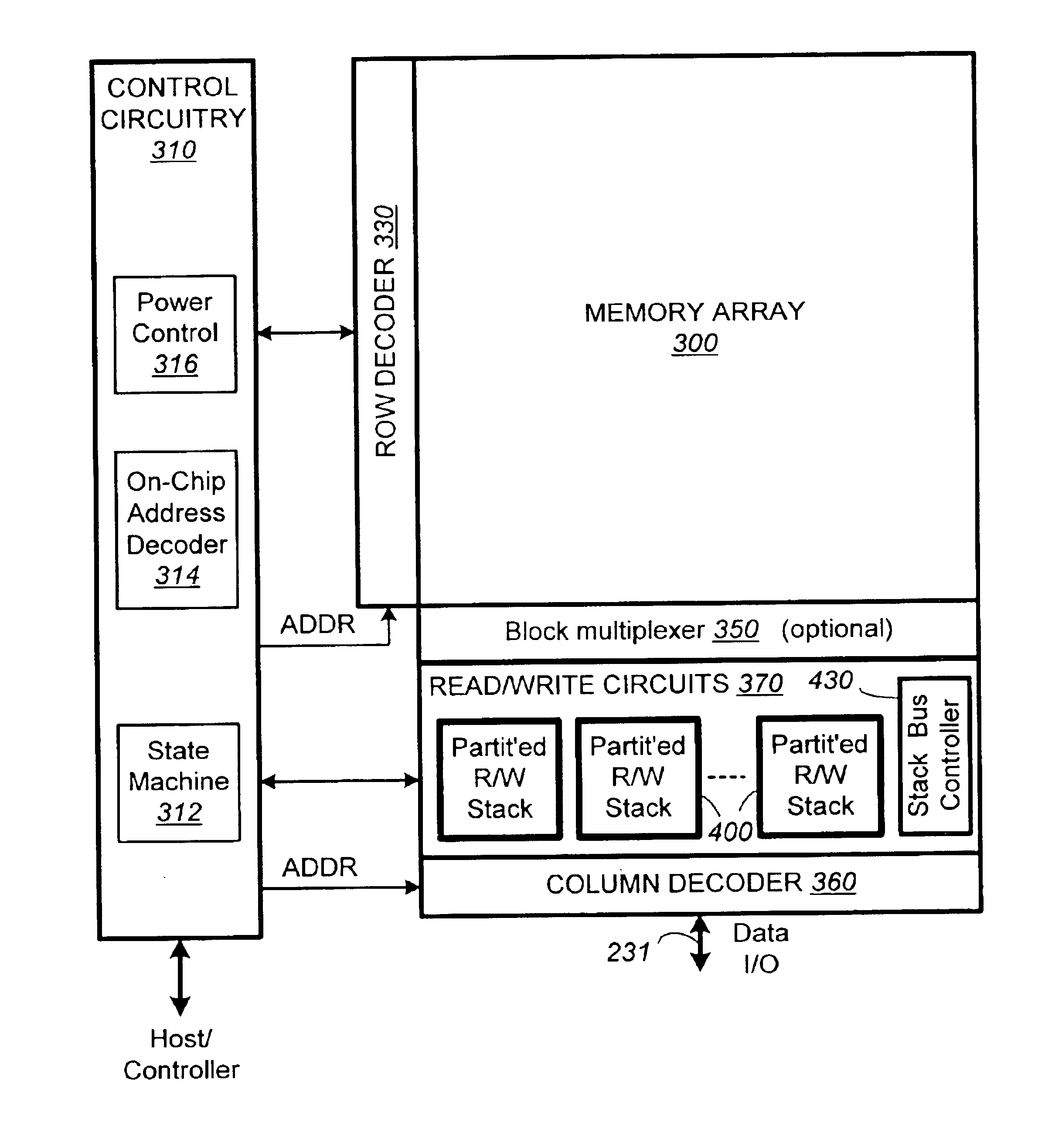
[0076]FIG. 7A is a schematic block diagram of an individual read / write module 200 partitioned into a core portion 210 and it common portion 220, according to a preferred embodiment of the present invention. The core portion 210 comprises a sense amplifier 212 that determines whether a conduction current in a connected bit line 211 is above or below a predetermined threshold level. As described in an earlier section, the connected bit line 211 enables access to the drain of an addressed memory cell in an array.

[0077]In one embodiment, the core portion 210 also includes a bit line latch 214. The bit line latch is used to set a voltage condition on the connected bit line 211. In one implementation, a predetermined state latched in the bit line latch will result in the connected bit line 211 being pulled to a state designating program inhibit (e.g., Vdd.) This feature is used for program inhibition as will be described later.

[0078]The common portion 220 comprises a processor 222, a set ...


PUM


Abstract

A non-volatile memory device capable of reading and writing a large number of memory cells with multiple read/write circuits in parallel has an architecture that reduces redundancy in the multiple read/write circuits to a minimum. The multiple read/write circuits are organized into a bank of similar stacks of components. Redundant circuits among each stack are factored out. In one aspect, a serial bus allows communication between components in each stack, thereby reducing the number of connections in a stack to a minimum. A bus controller sends control and timing signals to control the operation of the components and their interactions through the serial bus. In a preferred embodiment, the bus transactions of corresponding components in all the similar stacks are controlled simultaneously.

Description

FIELD OF THE INVENTION[0001]This invention relates generally to non-volatile semiconductor memory such as electrically erasable programmable read-only memory (EEPROM) and flash EEPROM, and specifically ones having highly compact and high performance write and read circuits.BACKGROUND OF THE INVENTION[0002]Solid-state memory capable of nonvolatile storage of charge, particularly in the form of EEPROM and flash EEPROM packaged as a small form factor card, has recently become the storage of choice in a variety of mobile and handheld devices, notably information appliances and consumer electronics products. Unlike RAM (random access memory) that is also solid-state memory, flash memory is non-volatile, retaining its stored data even after power is turned off. In spite of the higher cost, flash memory is increasingly being used in mass storage applications. Conventional mass storage, based on rotating magnetic medium such as hard drives and floppy disks, is unsuitable for the mobile and ...

Claims


Application Information

Patent Timeline
Patent Type & Authority Patents(United States)
IPC IPC(8): G11C16/10G11C7/10G11C16/26G11C16/06
CPCG11C7/1006G11C16/26G11C16/10
Inventor CERNEA, RAUL-ADRIAN
Owner INNOVATIVE MEMORY SYST INC
Why Eureka
Try Eureka