Use of ammonia for etching organic low-k dielectrics

a dielectric and organic technology, applied in the field of semiconductor wafer etching of organic low-k dielectrics, can solve the problems of slow operation of semiconductor devices, insufficient reduction of coupling capacitances, and each of these is, however, less than ideal, and achieves a higher degree of selectivity and etch ra

Inactive Publication Date: 2005-05-17
LAM RES CORP
View PDF21 Cites 19 Cited by
  • Summary
  • Abstract
  • Description
  • Claims
  • Application Information

AI Technical Summary

Benefits of technology

[0031]The present invention teaches a process chemistry utilizing ammonia, NH3, as an active etchant for etching features in wafers incorporating organic low-k dielectrics. The process results in significantly higher etch rates than previous N2 / H2 processes and which avoids the previously discussed problems with RIE lag and especially profile control. The process exhibits a much higher degree of selectivity between organic low-k dielectrics and commonly utilized hard mask materials. The process disclosed by the present invention enables a more stable etch plasma over a wider band of pressure and power operations than current N2 / H2 processes. The process disclosed herein is capable of being performed in situ within the fabrication equipment utilized to form the wafer, and is capable of implementation on a wide variety of existing integrated circuit manufacturing equipment. The ammonia etchant not only etches the organic low-k dielectric, but also removes the photoresist from the surface of the wafer.

Problems solved by technology

This introduces an increased level of coupling capacitance to the circuit, which has the drawback of slowing the operation of the semiconductor device.
Dielectric layers formed of SiO2 do not reduce the coupling capacitances sufficiently to levels required for increasing device densities and operating frequencies.
Each of these is, however, less than ideal.
Hydrogen-based etching processes, e.g.: N2 / H2 processes, are less than ideal for etching organic low-k dielectrics, particularly for etching the high-density features required in current sub-0.18 micron devices.
First, current N2 / H2 processes offer generally slow etch rates and poor profile control of the etched features: bowing and re-entrant etch profiles are particular problems.
Another problem relates to high aspect ratio features having differing sizes, which features are etched concurrently.
Another problem with known N2 / H2 chemistries is that they have generally poor selectivity with respect to the oxides and nitrides commonly used as hard masks during etching.
Another problem with N2 / H2 plasmas is that in general they are stable only over fairly narrow ranges of pressure and power as a result of the high ionization potential of N2.
Finally, etching of organic low-k dielectrics with known N2 / H2 processes is slow.
This leads to reduced wafer throughput and increased cost of ownership of processing equipment for the integrated circuit manufacturer.
O2 / N2 etch systems tend to possess much faster etch rates than N2 / H2 systems, but are especially prone to bowing and can degrade the dielectric constant of the low-k dielectric.
More troubling, they introduce a significant new problem, especially when utilized in conjunction with the manufacture of integrated circuit devices that incorporate copper.
Where copper in such devices is exposed to the etching environment, the use of an oxygen plasma often results in damage to the copper lines by generating copper-containing residue, which may deposit on the trench and via sidewalls causing copper contamination of the dielectric materials.
Eventual migration of the copper to the transistor level of the device leads to failure of the device due to copper poisoning.
This of course would result in lower process times and higher throughput.

Method used


Image

  • Use of ammonia for etching organic low-k dielectrics
  • Use of ammonia for etching organic low-k dielectrics
  • Use of ammonia for etching organic low-k dielectrics

Examples


Embodiment Construction

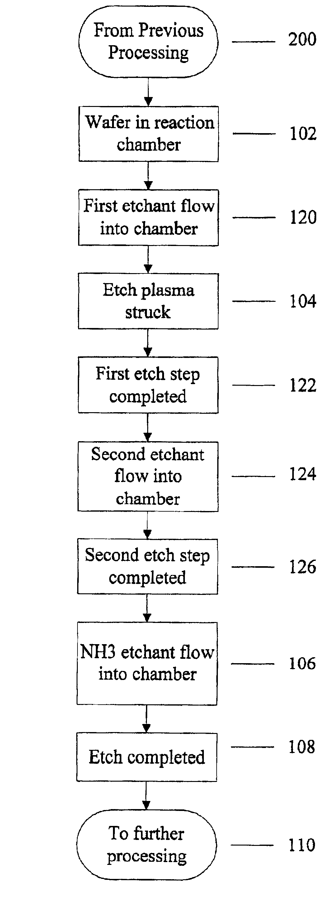
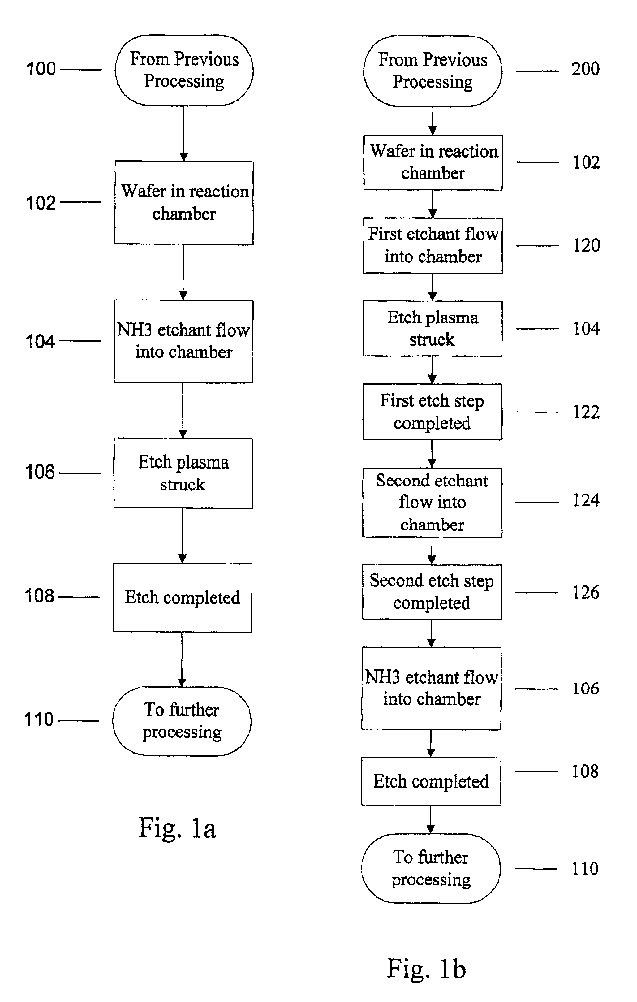
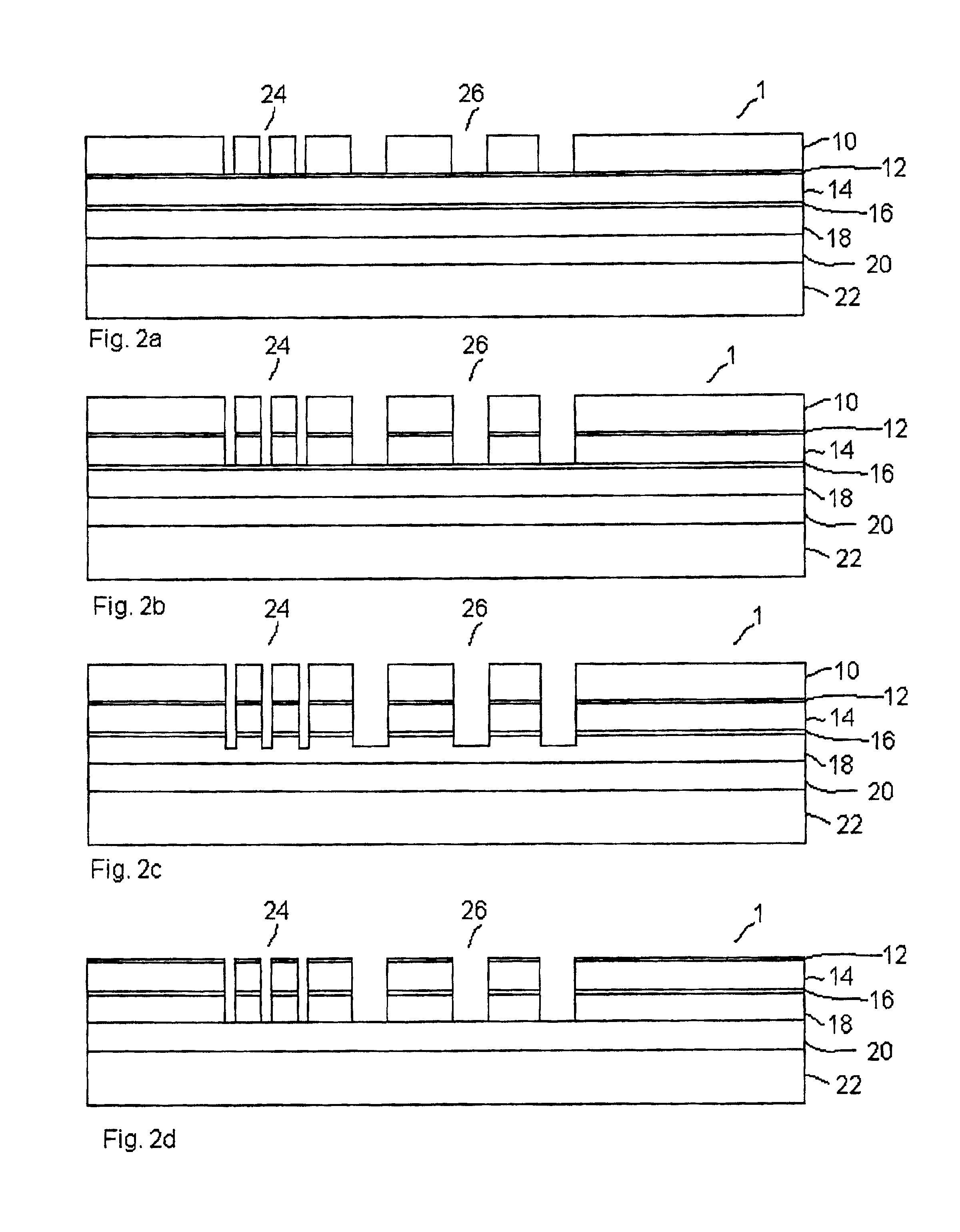
[0042]The present invention teaches a novel etch chemistry for etching a wide variety of feature sizes and shapes in wafers incorporating organic low-k dielectrics. The methodology taught herein results in minimal RIE lag, minimal bowing of the trenches and vias formed by the etch process, good etch profiles, and good etch uniformity across the wafer.

[0043]In order to etch a variety of features, including but specifically not limited to trenches and vias, in wafers including organic low-k dielectric layers the present invention implements ammonia as an etchant.

[0044]Having reference to FIG. 1a, in order to practice the process, 100, of the present invention a wafer is situated within a reaction vessel capable of forming an etch plasma. This reaction vessel or chamber may be an item of single purpose etching equipment, or may be a multiple purpose wafer processing system. One equipment particularly well suited for practicing the present invention is the Exelan™ dry etch system, avail...


PUM

PropertyMeasurementUnit
bias poweraaaaaaaaaa
temperatureaaaaaaaaaa

Abstract

Method for etching organic low-k dielectric using ammonia, NH3, as an active etchant. Processes using ammonia results in at least double the etch rate of organic low-k dielectric materials than processes using N2 / H2 chemistries, at similar process conditions. The difference is due to the much lower ionization potential of NH3 versus N2 in the process chemistry, which results in significantly higher plasma densities and etchant concentrations at similar process conditions.

Description

RELATED APPLICATIONS[0001]This application is also related to the commonly assigned U.S. patent application Ser. No. 09 / 781,185 entitled UNIQUE PROCESS CHEMISTRY FOR ETCHING ORGANIC LOW-K MATERIALS, by Helen H. Zhu, filed concurrently herewith and incorporated herein by reference.[0002]This application is related to the commonly assigned U.S. patent application Ser. No. 09 / 782,678 entitled POST-ETCH PHOTORESIST STRIP WITH O2 AND NH3 FOR ORGANOSILICATF GLASS LOW-K DIELECTRIC ETCH APPLICATIONS, by Rao V. Annapragada et al. filed concurrently herewith and incorporated herein by reference.[0003]This application is also related to the commonly assigned U.S. patent application Ser. No. 09 / 782,437 entitled USE OF HYDROCARBON ADDITION FOR THE ELIMINATION OF MICROMASKING DURING ETCHING OF ORGANIC LOW-K DIELECTRICS, by Chok W. Ho, filed concurrently herewith and incorporated herein by reference.FIELD OF THE INVENTION[0004]The present invention relates to semiconductor manufacture. More partic...

Claims


Application Information

Patent Timeline
Patent Type & Authority Patents(United States)
IPC IPC(8): B44C1/22C03C15/00C23F1/00H01L21/02H01L21/302H01L21/70H01L21/306H01L21/311H01L21/768
CPCH01L21/31144H01L21/31138H01L21/3065
Inventor HO, CHOK W.TANG, KUO-LUNGLEE, CHUNG-JU
Owner LAM RES CORP
Why Eureka
Try Eureka