Growth of III-nitride films on mismatched substrates without conventional low temperature nucleation layers

a technology of iiinitride and substrate, which is applied in the direction of polycrystalline material growth, crystal growth process, chemically reactive gas growth, etc., can solve the problems of increased accumulation probability, unsatisfactory use of low temperature nucleation layer, and difficult fabrication of thick, flat, defect-free iii-nitride layers, etc., to reduce the reaction between the group v precursor and the substrate, reduce the ratio, and eliminate the effect of temperature cycling

Active Publication Date: 2005-05-31
LUMILEDS
View PDF33 Cites 80 Cited by
  • Summary
  • Abstract
  • Description
  • Claims
  • Application Information

AI Technical Summary

Benefits of technology

[0009]In accordance with embodiments of the present invention, a method of forming a light emitting device includes providing a sapphire substrate, growing an Al1−xGaxN first layer by vapor deposition on the substrate at a temperature between about 1000° C. and about 1180° C., and growing a III-nitride second layer overlying the first layer. The first layer may have a thickness between about 500 angstroms and about 5000 angstroms. In some embodiments, reaction between the group V precursor and the substrate is reduced by starting with a low molar ratio of group V precursor to group III precursor, then increasing the ratio during growth of the first layer, or by using nitrogen as an ambient gas.
[0010]The use of a high temperature nucleation layer according to embodiments of the present invention is preferable to a low temperature nucleation layer because it may eliminate the temperature cycling, growth pause, and additional processing required for low temperature nucleation layers, and because it eliminates problems with uniformity due to the narrow thickness and temperature regimes required by low temperature nucleation layers.

Problems solved by technology

Since III-nitride substrates are generally not commercially available, III-nitride devices are often fabricated on substrates such as sapphire and SiC, which are referred to as “mismatched” because of differences in lattice constant and thermal expansion coefficients between these substrates and III-nitride layers.
The differences in lattice constant and thermal expansion coefficient cause strain which makes the fabrication of thick, flat, defect-free III-nitride layers difficult.
The use of low temperature nucleation layers is not ideal for several reasons.
Such temperature cycling is time consuming and therefore increases the likelihood of the accumulation of contaminants on the wafer surface that can affect yield or device performance.
Deviations from the desired heating pattern can cause poor device performance or poor yields.
Further, the materials quality of layers grown over the low temperature nucleation layer and the performance of the resulting device is sensitive to the thickness of the nucleation layer and the growth temperature of the nucleation layer.
The thickness and temperature regimes that yield acceptable device performance can be narrow, making it difficult to maintain the required thickness and temperature regimes across the wafer and resulting in poor yield.
Such additional processing increases the time and cost of fabrication and the risk of poor yield or poor device performance.
Ohba's method of fabricating a high temperature nucleation layer is undesirable because it requires high temperature growth and a growth pause in order to perform the anneal.

Method used


Image

  • Growth of III-nitride films on mismatched substrates without conventional low temperature nucleation layers
  • Growth of III-nitride films on mismatched substrates without conventional low temperature nucleation layers
  • Growth of III-nitride films on mismatched substrates without conventional low temperature nucleation layers

Examples


Embodiment Construction

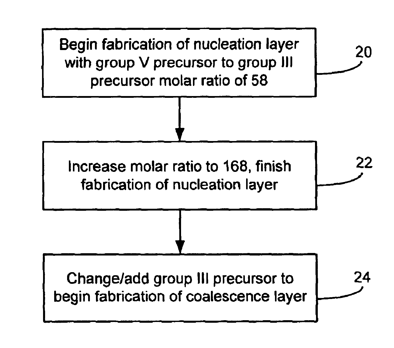
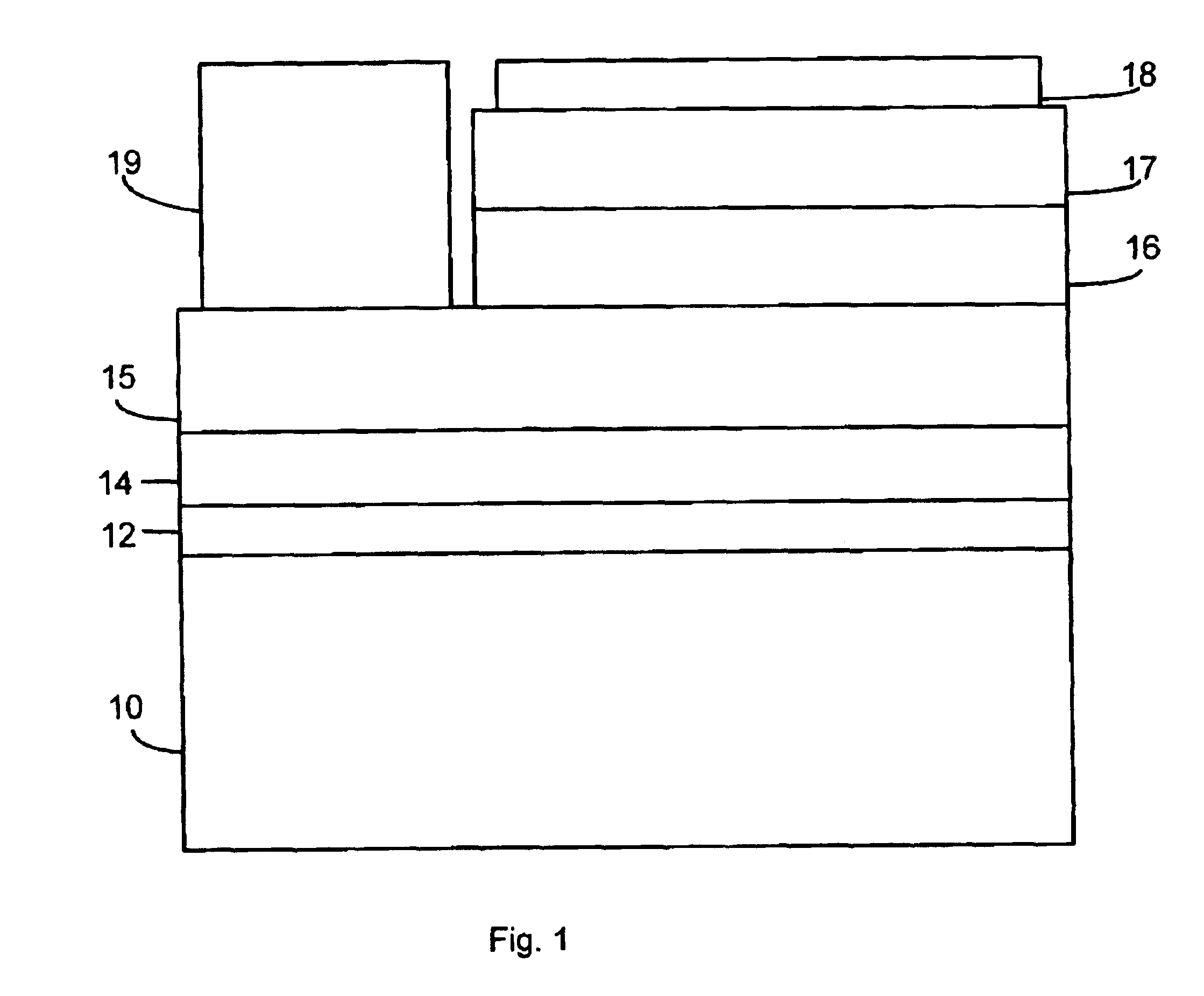
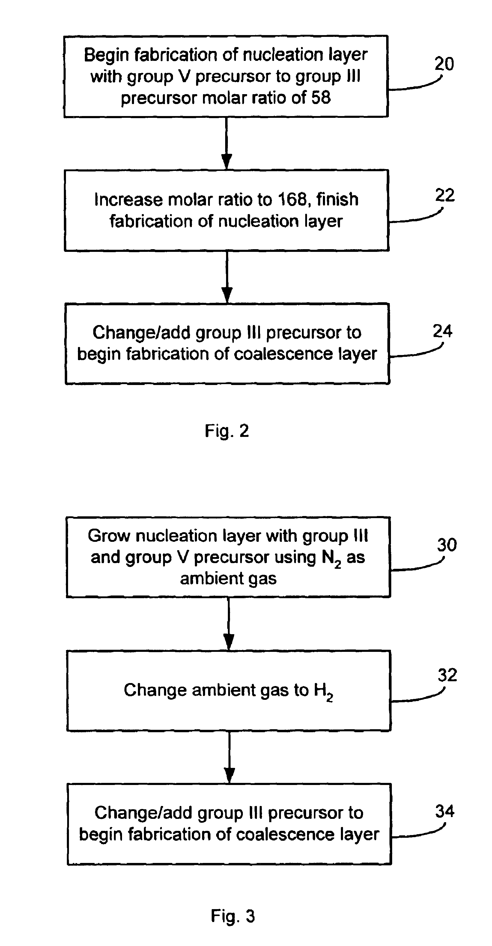
[0016]FIG. 1 illustrates a device according to an embodiment of the present invention. A high temperature nucleation layer 12 is formed over sapphire substrate 10. A coalescence layer 14 is then formed over nucleation layer 12, followed by an n-type region 15, an active region 16, and a p-type region 17. Each of n-type region 15, active region 16, and p-type region 17 may contain multiple layers of the same or different thickness, composition, and dopant concentration. In addition, n-type region 15 may contain one or more p-type layers, active region 16 may contain one or more n- or p-type layers, and p-type region 17 may contain one or more n-type layer. A portion of active region 16 and p-type region 17 are etched away to expose a portion of n-type region 15 on which n-contact 19 is formed. P-contact 18 is formed on p-type region 17. Contacts 18 and 19 may be reflective, such that light is extracted from the device through substrate 10, or transparent, such that light is extracted...


PUM

PropertyMeasurementUnit
thicknessaaaaaaaaaa
thicknessaaaaaaaaaa
temperatureaaaaaaaaaa

Abstract

A method of forming a light emitting device includes providing a sapphire substrate, growing an Al1−xGaxN first layer by vapor deposition on the substrate at a temperature between about 1000° C. and about 1180° C., and growing a III-nitride second layer overlying the first layer. The first layer may have a thickness between about 500 angstroms and about 5000 angstroms. In some embodiments, reaction between the group V precursor and the substrate is reduced by starting with a low molar ratio of group V precursor to group III precursor, then increasing the ratio during growth of the first layer, or by using nitrogen as an ambient gas.

Description

BACKGROUND[0001]1. Field of Invention[0002]This invention relates generally to the growth of III-nitride films on mismatched substrates.[0003]2. Description of Related Art[0004]Semiconductor light-emitting devices (LEDs) are among the most efficient light sources currently available. Materials systems currently of interest in the manufacture of high-brightness LEDs capable of operation across the visible spectrum include Group III-V semiconductors, particularly binary, ternary, and quaternary alloys of gallium, aluminum, indium, and nitrogen, also referred to as III-nitride materials. Typically, III-nitride light emitting devices are fabricated by epitaxially growing a stack of semiconductor layers of different compositions and dopant concentrations on a sapphire, silicon carbide, or III-nitride substrate by metal-organic chemical vapor deposition (MOCVD), molecular beam epitaxy (MBE), or other epitaxial techniques. The stack often includes one or more n-type layers doped with, for ...

Claims


Application Information

Patent Timeline
Patent Type & Authority Patents(United States)
IPC IPC(8): C30B25/02H01L21/02H01L21/20H01L21/205H01L33/00
CPCC30B25/02C30B29/403C30B29/406H01L21/0242H01L33/007H01L21/0254H01L21/02576H01L21/0262H01L21/02458
Inventor KOBAYASHI, JUNKOGOETZ, WERNER K.
Owner LUMILEDS
Why Eureka
Try Eureka