Method and apparatus for producing semiconductor device

a semiconductor and device technology, applied in the field of semiconductor device production methods and apparatuses, can solve the problems of difficult to obtain pmos tft, amorphous silicon cannot be used to produce p-channel tft, and the tft is not available to the tfts

Inactive Publication Date: 2005-06-07
SEMICON ENERGY LAB CO LTD
View PDF30 Cites 64 Cited by
  • Summary
  • Abstract
  • Description
  • Claims
  • Application Information

AI Technical Summary

Benefits of technology

[0085]The present invention is characterized in that, in order to correct the warp of the glass substrate flatly, the glass substrate is sucked on a flat surface of a stage having the flat surface, the peripheral portion of the glass substrate is pressed (pressurized), or the like. Also, the present invention is characterized in that such a flattening and correcting means is added to the stage of the laser annealing unit.
[0086]According to the present invention, there is provided a laser annealing method including the steps of flattening a glass substrate on a stage and mounting the former on the latter, and irradiating a linear laser beam on the surface to be irradiated on the glass substrate in a scanning manner to conduct the laser annealing.
[0087]According to the present invention, there is provided a laser annealing method including the steps of crystallizing an amorphous silicon film formed on a glass substrate by heating into a crystalline silicon film, flattening the glass substrate on the stage and mounting the former on the latter, and irradiating a linear laser beam on the crystalline silicon film in a scanning manner to conduct the laser annealing.
[0088]According to the present invention, there is provided a laser annealing method including the steps of crystallizing an amorphous silicon film formed on a glass substrate by heating into a crystalline silicon film, mounting the glass substrate on a stage having a flat surface in such a manner that the lower surface of the glass substrate is in close contact with the flat surface of the stage, and irradiating a linear laser beam on the crystalline silicon film in a scanning manner to conduct the laser annealing.
[0089]According to the present invention, there is provided a laser annealing method including the steps of crystallizing an amorphous silicon film formed on a glass substrate by heating into a crystalline silicon film, mounting the glass substrate on a stage having a flat surface in such a manner that the lower surface of the glass substrate is sucked with the flat surface of the stage under vapor, and irradiating a linear laser beam on the crystalline silicon film in a scanning manner to conduct the laser annealing.
[0090]According to the present invention, there is provided a laser annealing method including the steps of crystallizing an amorphous silicon film formed on a glass substrate by heating into a crystalline silicon film, mounting the glass substrate on a stage having a flat surface in such a manner that the lower surface of the glass substrate is in close contact with the flat surface of the stage by pressing the peripheral portion of the upper surface of the glass substrate, and irradiating a linear laser beam on the crystalline silicon film in a scanning manner to conduct the laser annealing.

Problems solved by technology

In general, the electric field mobility of a semiconductor which is in an amorphous state is small, and therefore not available to the TFTs that require a high speed operation.
Also, the amorphous silicon cannot be used to produce a p-channel TFT (PMOS TFT) since the p-type electric field mobility of the amorphous silicon is remarkably small, and thus a complementary MOS circuit (CMOS) cannot be formed by the combination of the p-channel TFT and an n-channel TFT (NMOS TFT).
However, in the event of using a glass substrate which is inexpensive and rich in processability as an insulating substrate, it is extremely difficult to obtain, by only annealing, a crystalline silicon film which is satisfactorily high in electric field mobility (high to the degree that the CMOS circuit can be formed).
When the pixel matrix that constitutes the pixel portion of a liquid crystal display has the distribution of threshold voltages shown in FIG. 2, the display state becomes nonuniform, resulting in a defective image.

Method used


Image

  • Method and apparatus for producing semiconductor device
  • Method and apparatus for producing semiconductor device
  • Method and apparatus for producing semiconductor device

Examples


first embodiment

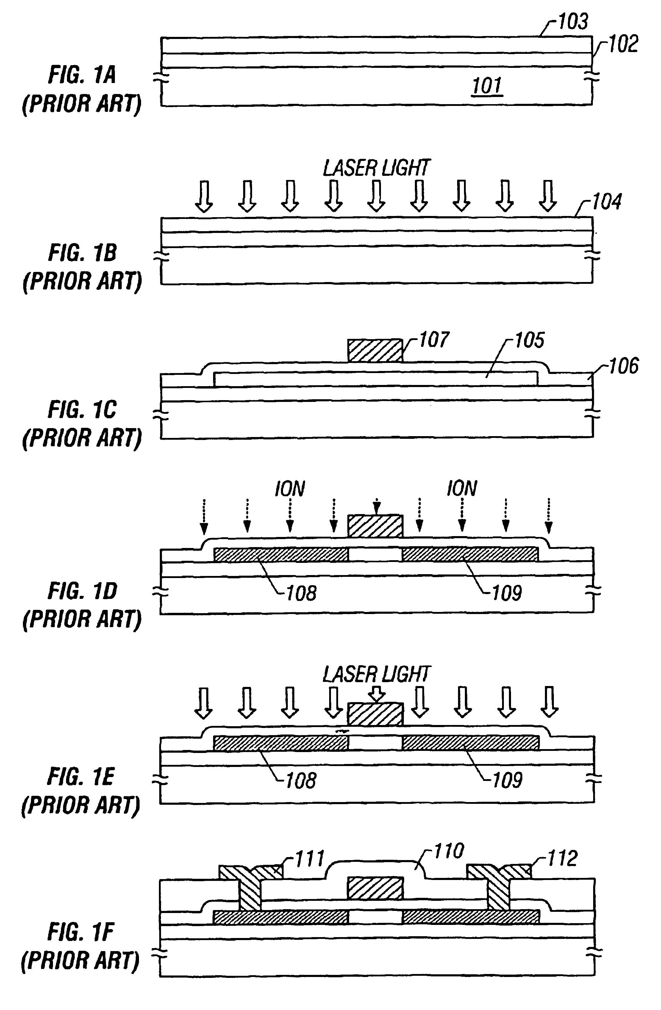
[0126]FIGS. 1A to 1F show a process of producing a thin film transistor (TFT) in accordance with a first embodiment.

[0127]An under silicon oxide film 102 having a thickness of 2000 Å is formed on a glass substrate (in this embodiment, using a Corning 7059 of 100 mm square), and an amorphous silicon film 103 having a thickness of 500 Å is formed sequentially on the under silicon oxide film 102 by plasma CVD.

[0128]Then, in order to add nickel as a catalytic element that promotes crystallization, nickel acetate aqueous solution of 10 ppm is coated on the surface of silicon, and nickel acetate layer not shown is formed through the spin coating technique.

[0129]It is more preferable that a surface active agent is added to the nickel acetate aqueous solution. Since the nickel acetate layer is very thin, although it is not limited to a film shape, it does not suffer from a problem in the subsequent process (FIG. 1A).

[0130]Then, the glass substrate 101 is located on a stage having a surface ...

second embodiment

[0153]A second embodiment will be described with reference to FIGS. 1A to 1F. An under silicon oxide film 102 having a thickness of 2000 Å is formed on a glass substrate 101 (In this embodiment, there is used a Corning 1737 of 400×500 mm square and 0.7 mm thickness. Another glass substrate such as Corning 7059, OA2, NA45, etc., may be used.), and an amorphous silicon film 103 having a thickness of 500 Å is formed sequentially on the under silicon oxide film 102 by plasma CVD.

[0154]Then, nickel acetate aqueous solution of 10 ppm is coated on the surface of silicon, and a nickel acetate layer not shown is formed by spin coating.

[0155]It is more preferable that a surface active agent is added to the nickel acetate aqueous solution. Since the nickel acetate layer is very thin, although it is not necessarily to be in a film shape, it does not suffer from any problem in the subsequent process (FIG. 1A).

[0156]Then, the glass substrate 101 is thermally annealed at 550° C. for four hours, to...

third embodiment

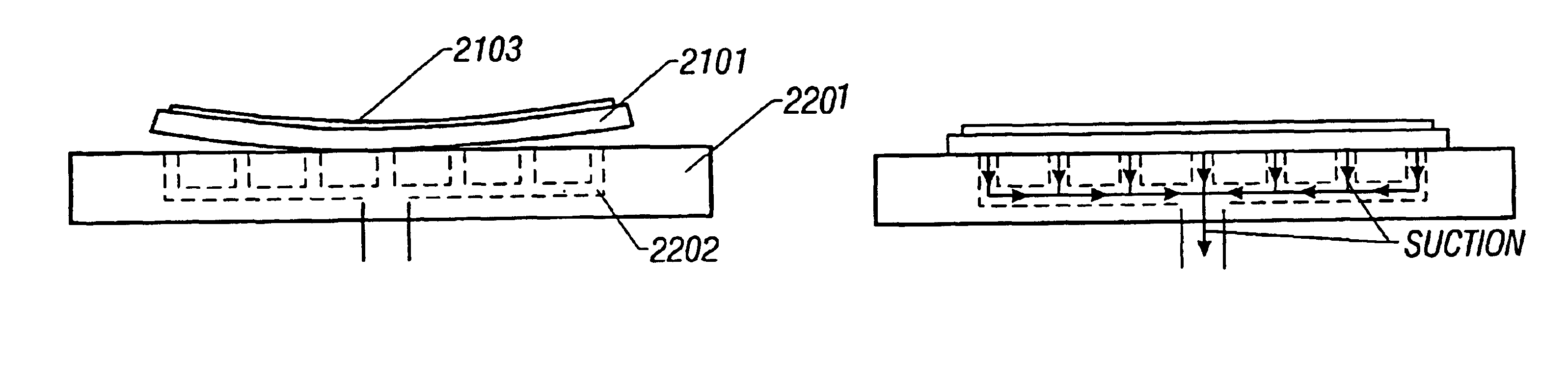
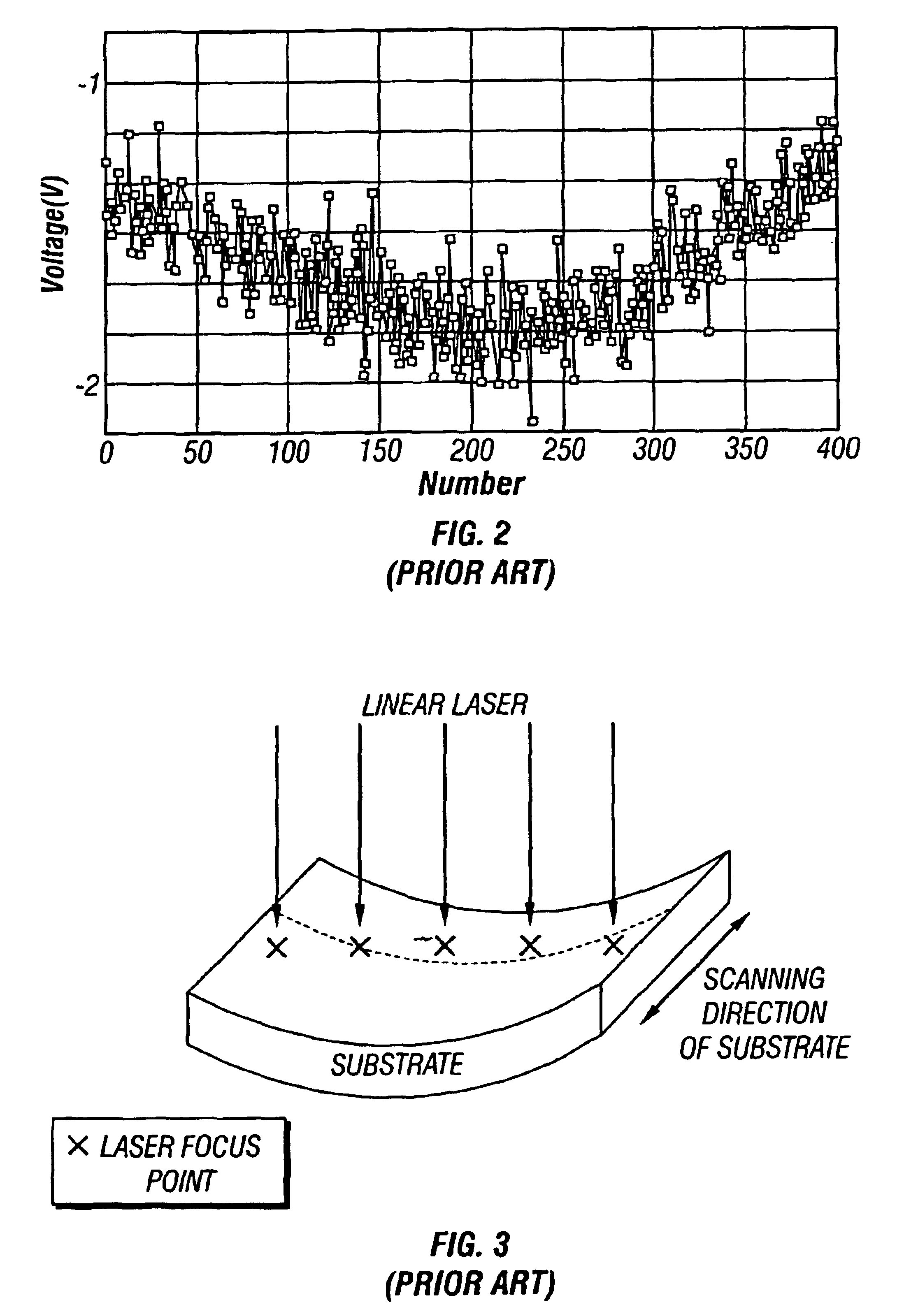
[0197]Although in the second embodiment, the glass substrate 101 of 400×500 mm square is used, in a third embodiment, Corning 7059 of 100 mm square is used for a glass substrate. Hence, in flattening the glass substrate which has been subjected to the crystallizing process, the shape of a stage on which the glass substrate shown in FIG. 6A is mounted may be of the inverse U-shape type convex curved surface which is curved in one direction.

[0198]The glass substrate is put on the stage having the inverse U-shape type convex curved surface, and an appropriate heat is applied to the glass substrate. Then, the glass substrate is deformed along the stage by self-weight and heat. In this situation, when the glass substrate is cooled, the silicon film formed on the substrate contracts more sharply than the glass substrate, with the result that an extremely flat glass substrate can be obtained.

[0199]Thereafter, a TFT is fabricated in the same manner as that of the first embodiment.

[0200]The ...


PUM

PropertyMeasurementUnit
lengthaaaaaaaaaa
surface roughnessaaaaaaaaaa
lengthaaaaaaaaaa

Abstract

A liquid crystal display device is manufactured by first forming a crystalline semiconductor film 2103, of silicon for example, over an insulating substrate 2101, such as glass. The substrate is warped in the process. The warpage is corrected by suction against a stage 2201. The film crystallinity is enhanced by scanning with a linear laser beam.

Description

[0001]This is a divisional of U.S. application Ser. No. 08 / 683,722, filed Jul. 18, 1996, now U.S. Pat. No. 5,907,770.BACKGROUND OF THE INVENTION[0002]1. Field of the Invention[0003]The present invention relates to a method and an apparatus for producing a semiconductor device which is capable of obtaining a crystalline silicon film high in uniformity by improving the flatness of a glass substrate during producing an insulated gate semiconductor device such as a thin film transistor (TFT) formed using a non-single crystal silicon film which is formed on the substrate, or other semiconductor devices. In particularly, the present invention is useful in producing a semiconductor device formed on the glass substrate.[0004]2. Description of the Related Art[0005]In recent years, several researches have been made into insulated gate field effect transistors having a thin film-shaped active layer (so-called active region) on an insulated substrate, which are so-called TFT).[0006]Those TFTs a...

Claims


Application Information

Patent Timeline
Patent Type & Authority Patents(United States)
IPC IPC(8): H01L21/20H01L21/02B23K26/42C30B1/00C30B29/06H01L21/00H01L21/336H01L21/36H01L21/84
CPCB23K26/422C30B1/00C30B29/06H01L29/6675H01L21/02532H01L21/02672H01L21/02678H01L21/02686H01L21/02422Y10S117/904Y10T117/1008Y10T117/1004B23K26/702
Inventor YAMAZAKI, SHUNPEITANAKA, KOICHIRO
Owner SEMICON ENERGY LAB CO LTD
Why Eureka
Try Eureka