Method of manufacturing a semiconductor device

a manufacturing method and semiconductor technology, applied in the direction of coatings, transistors, chemical vapor deposition coatings, etc., can solve the problems of insufficient mobility to obtain sufficient current, insufficient operation speed, and particularly inferior current and mobility characteristics of single crystal transistors, so as to reduce the size of semiconductor devices and improve the tolerance against physical impact

Inactive Publication Date: 2005-06-21
SEMICON ENERGY LAB CO LTD
View PDF12 Cites 103 Cited by
  • Summary
  • Abstract
  • Description
  • Claims
  • Application Information

AI Technical Summary

Benefits of technology

[0010]It is possible that a semiconductor device has a controller, a CPU, and so on provided in addition to driver circuits such as a gate line driving circuit and a source line driving circuit. Then, it has been tried recently to form a controller and a CPU, which used to be formed from a single crystal silicon substrate, on a glass substrate together with driver circuits. In the same way as the driver circuits, it is possible to suppress the size of a semiconductor device remarkably and to improve tolerance against physical impact more if it becomes possible to form the controller and the CPU on the same substrate together with the pixel portion.
[0015]The present invention provides a technique for solving the above problem. It is an object of the present invention to provide a method of manufacturing a semiconductor device, which enables to improve on current and mobility of the polycrystal TFT without hindering high integration level.
[0026]Specifically, it is preferable that laser light is scanned with the scan speed less than 20 cm / sec to get a higher orientation ratio of {100} in a region in which an n-channel TFT is formed and laser light is scanned with the scan speed over 20 cm / sec to get a higher orientation ratio of {110} in a region in which an p-channel TFT is formed. As a result, it is possible to make not only the mobility but also on current get higher.
[0031]It is noted that it is possible to control the orientation ratios of {100} and {110} more effectively when, in addition to controlling the scan speed of laser light, it is selected if thermal crystallization with a catalytic element is performed or not.
[0042]In short, when a p-channel TFT is formed of the semiconductor film of the region 1 and an n-channel TFT is formed of the semiconductor film of the region 2, it is possible to improve not only mobility but also on current of the respective p-channel and n-channel TFFs without disturbing a high integration level.

Problems solved by technology

However, characteristics of the polycrystal TFT were not equal to characteristics of a MOS transistor (single crystal transistor) formed on a single crystal silicon substrate after all.
Due to existence of a defect in an interface between crystal grains (grain boundary), on current and mobility of the characteristics were especially inferior to the single crystal transistor.
Therefore, the mobility is not enough to obtain sufficient on current and the operation speed is insufficient when it is tried to manufacture integrated circuits such as a controller and a CPU from polycrysal TFTs.
It is, however, limited to reduce the size of the channel length L in terms of accuracy in an exposure technique.
Further, considering wiring resistance, it is indispensable that an integration level is high to some extent in integrated circuits such as a controller and a CPU, and therefore it is limited to arrange the layout of TFTs and wirings and it is not easy to extend the channel width W. Accordingly, it was limited to control W / L and it was difficult with only the control of W / L to acquire enough on current.

Method used


Image

  • Method of manufacturing a semiconductor device
  • Method of manufacturing a semiconductor device
  • Method of manufacturing a semiconductor device

Examples


embodiment mode 1

[Embodiment Mode 1]

[0063]In the present embodiment mode, there will be described a method of manufacturing a TFT, which combines, in addition to controlling the scan speed of laser light, controlling if thermal crystallization with a catalytic element is performed or not.

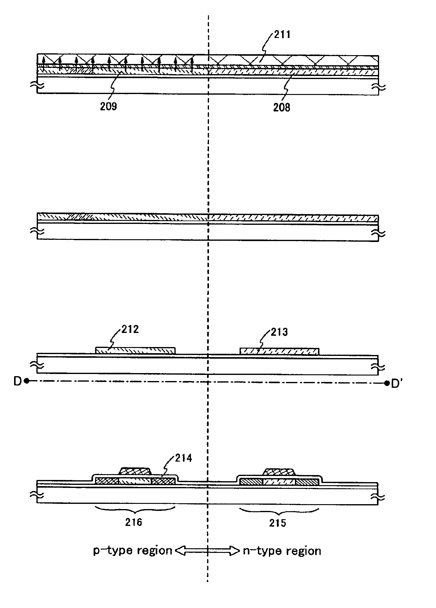
[0064]First, a base film 201 is formed by deposition on a substrate 200 as shown in FIG. 6A. As the substrate 200, a non-alkali glass substrate, represented by, for example, #1737 glass substrate produced by Corning corp. is used. In addition to the #1737 glass substrate, the barium borosilicate glass such as #7059 glass may be used as the substrate, and a quartz substrate, a silicon substrate, a metallic substrate, or a stainless steel substrate, which has an insulating film formed on the surface, may also be used. Also, a plastic substrate that has a heat resistance to a processing temperature in the present embodiment mode may be used.

[0065]The base film is formed of an insulating film such as a silicon oxide fil...

embodiment mode 2

[Embodiment Mode 2]

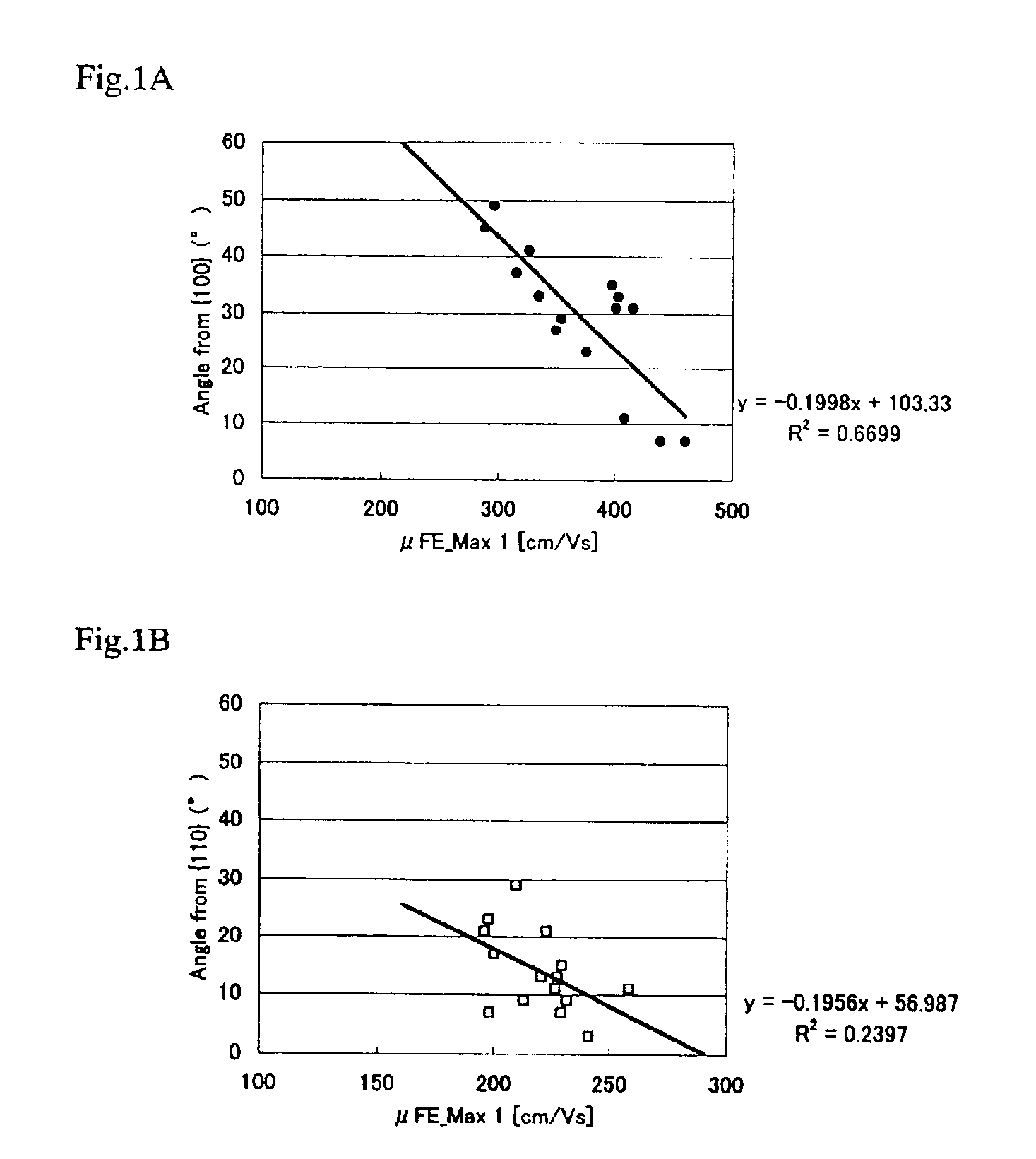
[0100]In the present embodiment mode, there will be described the case of irradiating laser light for crystallization after crystallization with a catalytic element in a perpendicular direction to a substrate (vertical growth) in a p-type region.

[0101]In each of FIGS. 9A and 9B, a mapping figure of an inverse pole figure of a plane direction in a crystal plane in a horizontal direction to a substrate is shown. Before irradiating laser light, a catalytic element is added to a semiconductor film and heat treatment is performed in FIG. 9A. In FIG. 9B, heat treatment is performed to a semiconductor film without adding a catalytic element.

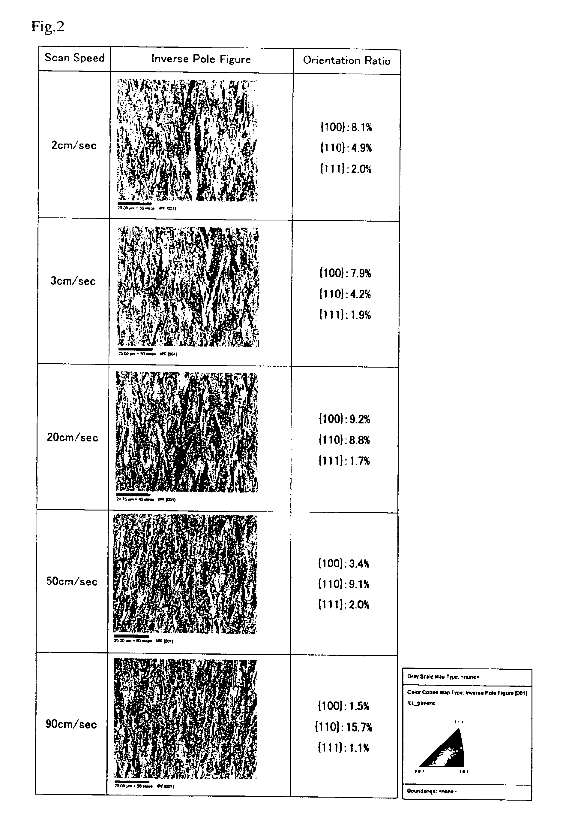
[0102]In FIGS. 9A and 9B, samples to which laser light is scanned in a horizontal direction to a substrate are used. In irradiating laser light, continuous emission Nd:YVO4 laser is used, the energy density is set to 10 MW / cm2, and the scan speed is 50 cm / sec. The film thickness of the semiconductor film is 150 nm. It is noted that an...

embodiment 1

[Embodiment 1]

[0136]In the present embodiment, a semiconductor display device, that is one of semiconductor devices manufactured in accordance with a manufacturing method of the present invention, is given as an example, and a scanning course of laser light in crystallization will be described.

[0137]FIG. 12A shows a canning course of laser light in irradiating laser light to an n-type region, and FIG. 12B shows a canning course of laser light in irradiating laser light to a p-type region. It is noted, in FIGS. 12A and 12B, that a semiconductor film 850 is formed on a substrate and broken lines show regions in which a pixel region 853, a source line driving circuit 854, a gate line driving circuit 855, an image signal processing circuit 856, a VRAM (Video Random Access Memory) 857, and a timing signal generating circuit 858 are respectively formed in the semiconductor film 850.

[0138]The VRAM 857 has a function of memorizing data that has image information input from the outside. The ...


PUM

PropertyMeasurementUnit
scan speedaaaaaaaaaa

Abstract

The present invention provides a manufacturing method of a semiconductor device, which is able to improve on-current and mobility of a polycrystal TFT without disturbing a high integration level, and also provide a semiconductor device obtained in accordance with the manufacturing method. The manufacturing method comprises steps of adding a catalytic element to a semiconductor film and heating the semiconductor film to form a more crystallized first region; forming a less crystallized second region than the first region; irradiating first laser light to the first region to form a more crystallized third region than the first region; irradiating second laser light to the second region to form a more crystallized fourth region than the second region; and patterning the third region to form a first island-shaped region and the fourth region to form a second island-shaped region, wherein the first laser light has the same energy density from the second laser light, and a scan speed of the first laser light is faster than that of the second laser light.

Description

BACKGROUND OF THE INVENTION[0001]1. Field of the Invention[0002]The present invention relates to a method of manufacturing a semiconductor device that has a semiconductor element, typically a thin film transistor (TFT), that has a semiconductor film crystallized on an insulating surface.[0003]2. Description of the Related Art[0004]In electronic devices such as a television, a personal computer, and a cellular phone, a display for displaying characters or images is indispensable as a means for recognizing information. In these days especially, a flat-type semiconductor display device (flat panel display), represented by a liquid crystal display device that utilizes the electro-optical character of liquid crystal, has actively been used.[0005]An active matrix driving method is known as one mode in the flat panel display. In the active matrix driving method, a TFT is provided in each pixel and image signals are in order written to perform a display of an image. The TFT is an essential ...

Claims


Application Information

Patent Timeline
Patent Type & Authority Patents(United States)
IPC IPC(8): H01L29/786H01L21/02H01L21/20H01L21/70H01L21/84H01L29/66H01L27/12H01L21/77
CPCH01L21/2022H01L21/2026H01L27/1285H01L29/78675H01L27/1277H01L27/12H01L21/02422H01L21/02532H01L21/02672H01L21/02683
Inventor TAKANO, TAMAE
Owner SEMICON ENERGY LAB CO LTD
Why Eureka
Try Eureka