Semiconductor device applying to the crystalline semiconductor film

Inactive Publication Date: 2005-06-21
SEMICON ENERGY LAB CO LTD
View PDF86 Cites 22 Cited by
  • Summary
  • Abstract
  • Description
  • Claims
  • Application Information

AI Technical Summary

Benefits of technology

[0017]The present inventors paid attention to the fact that crystal growth conditions greatly depend on the width of a catalytic element introdu

Problems solved by technology

However, the catalytic element for promoting crystallization of the amorphous silicon film often deteriorates the characteristics of the TFT.
Besides, even if the catalytic element is removed in a step

Method used


Image

  • Semiconductor device applying to the crystalline semiconductor film
  • Semiconductor device applying to the crystalline semiconductor film
  • Semiconductor device applying to the crystalline semiconductor film

Examples


embodiment 1

[Embodiment 1]

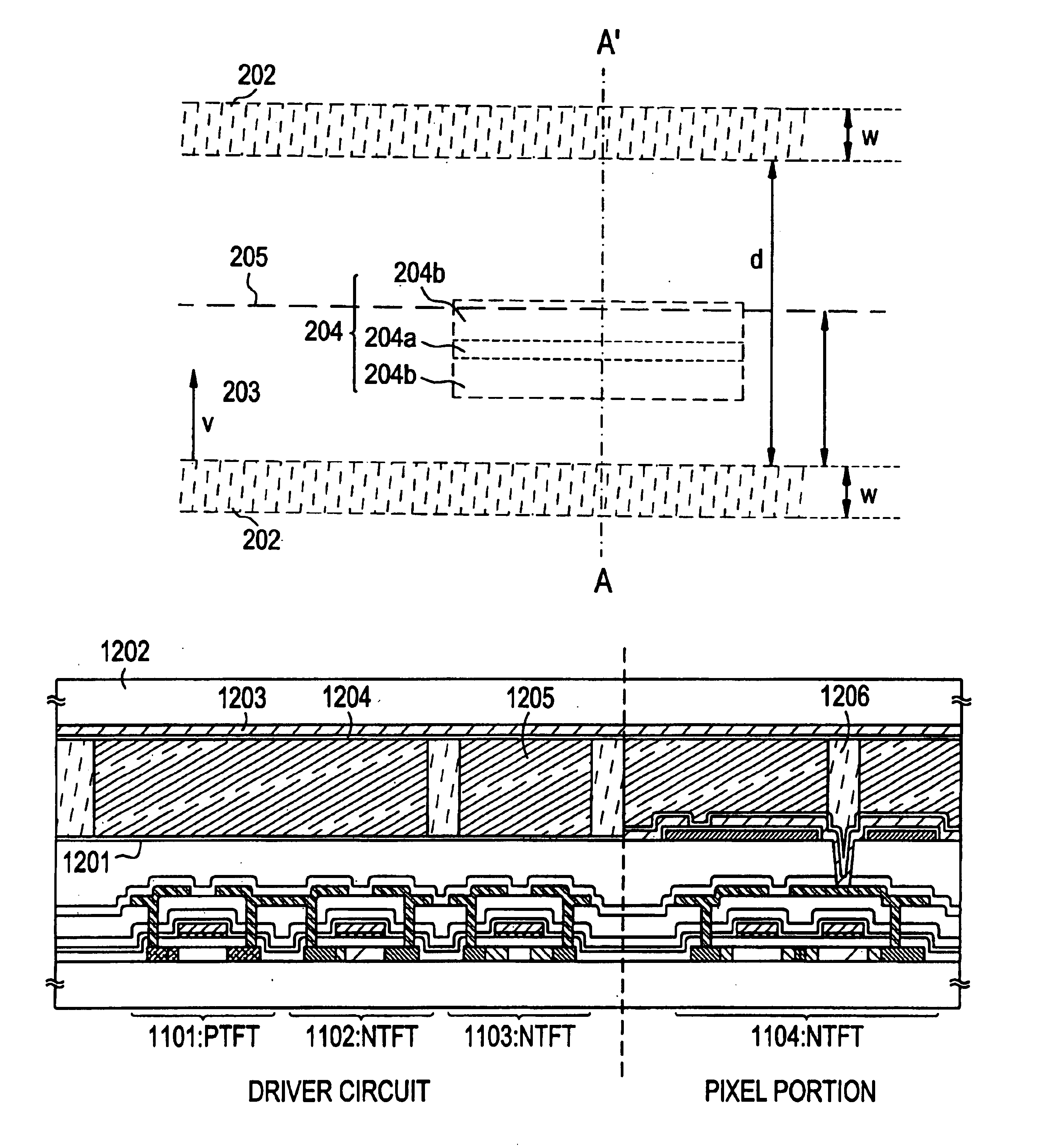
[0101]In this embodiment, with respect to the structure of the invention, a method of fabricating an active matrix type substrate in which a pixel portion and a CMOS circuit as a base of a driver circuit provided at a periphery thereof are formed at the same time, will be described with reference to FIGS. 8A to 14.

[0102]In FIG. 8A, it is desirable to use a glass substrate, a quartz substrate, or a silicon substrate as a substrate 801. In this embodiment, the quartz substrate was used. Other than those, a metal substrate or what is obtained by forming an insulating film on a stainless substrate may be used as the substrate. In the case of this embodiment, since heat resistance capable of withstanding a temperature of 800° C. or higher is required, as long as a substrate satisfies that, any substrate may be used.

[0103]A semiconductor film 802 having a thickness of 20 to 100 nm (preferably 40 to 80 nm) and comprising amorphous structure is formed on the surface of the sub...

embodiment 2

[Embodiment 2]

[0182]In this embodiment, a description will be made on a case where another means is used for reducing the catalytic element in the crystalline silicon film in the embodiment 1.

[0183]In the embodiment 1, although gettering for reducing a catalytic element in a crystalline silicon film is carried out by performing a heat treatment after a phosphorus element is selectively added, and gettering is carried out by performing a heat treatment in an oxidizing atmosphere including a halogen element, this embodiment shows an example in which after a gate electrode is formed, a phosphorus element is added, and a heat treatment at 500 to 650° C. for 2 to 16 hours is performed.

[0184]First, in accordance with the steps of the embodiment 1, the state of FIG. 10C was obtained. Next, phosphorus is added into an active layer with a gate electrode as a mask so that its concentration becomes 5×10¹⁸ to 1×10²⁰ atoms / cm3 (preferably 1×10¹⁹ to 5×10¹⁹ atoms / cm3). However, since the concentra...

embodiment 3

[Embodiment 3]

[0190]The crystal structure of an active layer that went through the processes up to the thermal oxidation process shown in FIG. 9A of Embodiment 1 is a unique crystal structure which has continuity in the crystal lattice. Its characteristics are described below.

[0191]The crystalline silicon film which was fabricated in accordance with the manufacturing processes of Embodiment 1 has a crystal structure in which a plurality of needle-like or column-like crystals are gathered and aligned when viewed microscopically. This may readily be confirmed through observation using TEM (transmission electron microscopy).

[0192]By using electron diffraction and X-ray diffraction, {110} plane was observed on its surface (where a channel is to be formed) as a principle orientated film though crystal axis was more or less shifted. As a result of thoroughly observing an electron diffraction photograph with a spot diameter of approximately 1.5 μm by the Applicant, it was confirmed that th...


PUM


Abstract

There is disclosed a semiconductor device and a method of fabricating the semiconductor device in which a heat treatment time required for crystal growth is shortened and a process is simplified. Two catalytic element introduction regions are arranged at both sides of one active layer and crystallization is made. A boundary portion where crystal growth from one catalytic element introduction region meets crystal growth from the other catalytic element introduction region is formed in a region which becomes a source region or drain region.

Description

BACKGROUND OF THE INVENTION[0001]1. Field of the Invention[0002]The present invention relates to a semiconductor device including a circuit constituted by thin film transistors (hereinafter referred to as TFTs) and a method of fabricating the same. For example, the invention relates to an electro-optical device typified by a liquid crystal display panel, and an electronic apparatus incorporating such an electro-optical device as a component.[0003]Note that in the present specification, the term “semiconductor device” indicates any devices capable of functioning by using semiconductor characteristics, and all of the electro-optical devices, semiconductor circuits, and electronic apparatuses are semiconductor devices.[0004]2. Description of the Related Art[0005]In recent years, attention has been paid to a technique to construct a thin film transistor (TFT) by using a semiconductor thin film (thickness of several to several hundreds nm) formed over a substrate having an insulating sur...

Claims


Application Information

Patent Timeline
IPC IPC(8): H01L21/336H01L29/786H01L21/02H01L21/20H01L21/70H01L21/84H01L29/66H01L27/12G02F1/13G02F1/1362G09G3/36G09G3/32G09G3/30H01L27/32H01L27/28G02F1/136G02F1/1368H01L21/77H01L29/04
CPCH01L27/1277H01L21/2022H01L27/12H01L29/04H01L29/66757H01L29/78624H01L29/78645H01L29/78675H01L27/1248G02F1/13454G09G3/3225G09G3/3233G09G3/3648G09G2300/0842G09G2300/0861H01L27/3244G09G3/30H01L27/1255H01L21/02672H01L21/02532H10K59/12
Inventor KOKUBO, CHIHOYAMAGATA, HIROKAZUYAMAZAKI, SHUNPEI
Owner SEMICON ENERGY LAB CO LTD
Why Eureka
Try Eureka