[0009]It is well known that carbon (C) can serves as a retardant of
dopant diffusion in both Si and SiGe materials and devices. For example, H. J. Osten et. al, in the paper entitled “
Carbon Doped SiGe
Heterojunction Bipolar Transistors for
High Frequency Applications, IEEE BCTM 7.1, 1999, pp 109-116, which is incorporated herein by reference, have shown that low carbon concentrations (<1020 atom / cm3) can significantly suppress
boron out-
diffusion without affecting the strain or band alignment of carbon-rich SiGe:B
layers in order to achieve high performance SiGe
heterojunction bipolar transistors. Similarly, Rucker et. al., in a paper entitled “
Dopant Diffusion in C-doped Si and SiGe:
Physical Model and Experimental
Verification”,IEDM, 1999, pp345-348, which is incorporated herein by reference, have further shown that
carbon doping can be used to suppress P
diffusion as well, in addition to suppressing the transient enhanced diffusion (TED) behavior of B. With appropriate techniques, such as UHV-CVD, during Si deposition C can be distinctly incorporated to a few percent into crystalline, or polycrystalline Si films without any
residual oxygen contamination often associated with other
carbon doping or growth techniques. The resulting material Si:C is practically a stopping layer for diffusing electrically active impurities, such as
boron or phosphorous. The technique can also be used when C is incorporated into SiGe during deposition, giving SiGe:C films. With UHV-CVD one can deposit ultra-thin, device quality
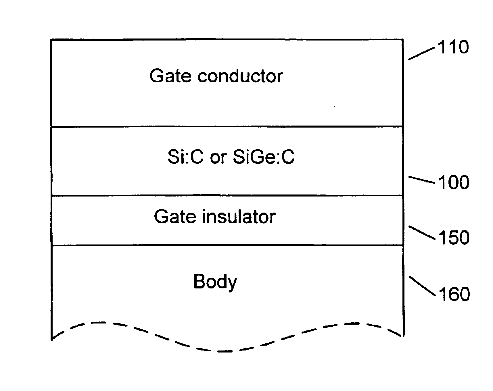
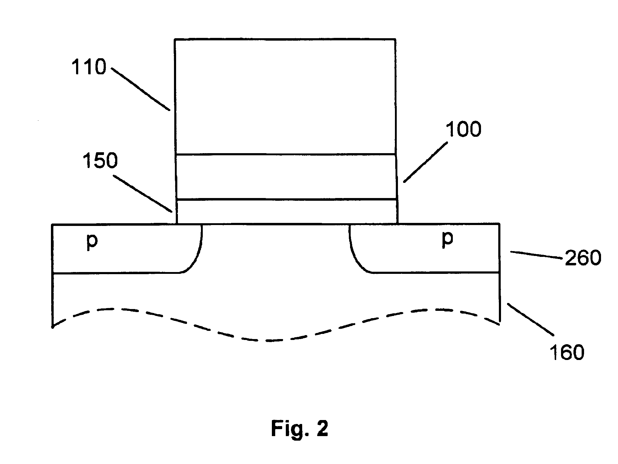
layers of Si:C or SiGe:C up to approximately 10% of C content. Disposing such a dopant
barrier layer onto the gate insulator, prior to the deposition of the doped layer, has the desired effect of protecting the channel region underneath the gate insulator without upsetting the electrical properties of the device. Since from
etching behavior, or a patterning point of view the properties of Si:C and SiGe:C are almost the same as those of pure Si, the Si:C or SiGe:C layer would not need any special
processing, such as additional patterning, or
etching step beyond those typical of standard
MOSFET fabrication. The Si:C or SiGe:C can be deposited in
blanket, or borderless, manner just prior to the deposition of the bulk of the gate material, which is typically doped polysilicon. It is the objective of this invention to teach the prevention of dopant
impurity penetration of the gate insulator by depositing a Si:C or SiGe:C layer directly over the gate insulator to serve as the dopant
diffusion barrier.
[0022]The invention further teaches the devices hosted in the strained Si based
layers on insulators, which can operate from 400° K to 5° K, and teaches processors functioning with such devices. The high end of the approximate range, 400° K, although achievable with the high performance techniques disclosed herein, it is not the most preferable for the optimal FET performance. High performance is associated with strained device layers, and SOI technology, and also with low temperature operation. Device performance (for FET type devices) improves with decrease in temperature. To obtain the optimal performance of devices at low temperatures they have to be device-designed already for low temperature operation. Such device-designs, optimized for low temperature operation, are well known in the previous art. A desirable temperature range for low temperature high performance FET operation is between about 250° K and 70° K. This invention, by combining the device-designs for operation in the 400° K to 5° K range with the SOI technology and with the both tensilely and compressively strained device layers directly on the insulators aims at devices and processors of the utmost performance. Devices where the strained layers are directly on the insulators are especially suitable for low temperature operation due to their low
capacitance. Also, multifaceted gate devices have relatively large surfaces which helps decreasing source /
drain resistance, another
advantage for low temperature operation. An all cases where Shottky junction electrodes are utilized, as in several of the high performance devices disclosed herein, benefit from low temperature operation.

