Method for producing metal/ceramic bonding circuit board

a technology of metal/ceramic bonding and circuit board, which is applied in the direction of insulating substrate metal adhesion improvement, manufacturing tools, solventing apparatus, etc., can solve the problems of high cost, large number of processes, and inability to meet, and achieves low cost, small number of steps, and easy control of the sectional shape of metal/ceramic bonding circuit board

Inactive Publication Date: 2005-07-19
DOWA METALS & MINING CO LTD
View PDF28 Cites 22 Cited by
  • Summary
  • Abstract
  • Description
  • Claims
  • Application Information

AI Technical Summary

Benefits of technology

[0012]It is therefore an object of the present invention to eliminate the aforementioned problems and to provide a method for producing a metal / ceramic bonding circuit board, the method being capable of easily controlling the sectional shape of a metal / ceramic bonding circuit board by a smaller number of steps and at low costs and capable of producing a metal / ceramic bonding circuit board being more reliable with respect to thermal shock resistance and insulation performance.
[0013]It is another object of the present invention to provide a method for producing a metal / ceramic bonding circuit board, the method being capable of preventing shear drops from being caused from the top of a metal plate, capable of using chemicals which have smaller attacks on a ceramic substrate and which consider environment, and capable of simplifying facilities, such as waste solution treating facilities, and waste solution treatments.
[0014]In order to accomplish the aforementioned and other objects, the inventors have diligently studied and found that a method for producing a metal / ceramic bonding circuit board, wherein a metal plate is bonded to at least one side of a ceramic substrate via a brazing filler metal to form a circuit pattern, can easily control the sectional shape of a metal / ceramic bonding circuit board by a smaller number of steps and at low costs and can produce a metal / ceramic bonding circuit board being more reliable with respect to thermal shock resistance and insulation performance, if the method comprises the steps of: bonding a metal plate of a metal to at least one side of a ceramic substrate via a brazing filler metal; applying a resist on a predetermined portion of a surface of the metal plate to etch and remove an undesired portion of the metal plate to form a metal circuit portion; and removing an undesired portion of the brazing filler metal and a reaction product, which is produced by a reaction of the brazing filler metal with the ceramic substrate (or removing an undesired portion of the brazing filler metal and a reaction product, which is produced by a reaction of the brazing filler metal with the ceramic substrate, and etching a side portion of the metal circuit portion), while maintaining the resist, and thereafter, peeling off the resist to form a circuit pattern.

Problems solved by technology

However, in the case of the brazing and soldering method, this etchant can dissolve the metal plate, but it can not dissolve the brazing filler metal and the reaction product of the brazing filler metal with the ceramic substrate (the general term for the brazing filler metal and the reaction product will be hereinafter referred to as a “brazing filler metal and so forth”), so that the brazing filler metal and so forth remain between circuit patterns and / or on the edge face of the substrate.
Since the brazing filler metal and so forth are conductors, it is not possible to satisfy basic characteristics of a circuit board, which isolate the circuit patterns from each other and / or the surf ace and reverse of the board from each other.
In the former, it is possible to obtain the large protrusion of the brazing filler metal, but the number of processes is large and costs are high.
In the latter, the number of processes is the same as that in usual methods, but it is difficult to increase the protrusion of the brazing filler metal from the nature of the chemicals.
In addition, there are some cases where it is not possible to ignore attacks on the ceramic substrate from the nature of the chemicals.
Moreover, the top of the metal plate is also dissolved in the chemicals, which removes the brazing filler metal, to cause shear drops.
Therefore, a discrepancy is caused in the mounting of a chip, such as a semiconductor chip, so that there are some cases where it is required to carry out a design change, such as the increase of the size.
However, in conventional methods, it is difficult to control the length of the brazing filler metal and so forth protruding the edge portion of the metal plate (which will be hereinafter referred to as a “brazing filler metal protruding length”.
In particular, if the brazing filler metal protruding length is set to be long, the number of processes is larger than that in usual processes, so that production costs increase.
In addition, a brazing filler metal removing agent causes shear drops from the top of the metal plate to cause dimensional discrepancy when a chip, such as a semiconductor chip, is mounted thereon.
In addition, if chemicals containing hydrogen halide or ammonium halide, typically hydrofluoric acid, a mixed acid thereof or ammonium fluoride, are used as the brazing filler metal removing agent, there are some cases where the ceramic substrate is also corroded simultaneously with the removal of the brazing filler metal and so forth, so that characteristics with respect to reliability as the ceramic circuit board are deteriorated.
On the other hand, if the corrosion of the ceramic substrate is intended to be suppressed, there is some possibility that it is not possible to completely remove the brazing filler metal and so forth between circuit patterns, so that the brazing filler metal and so forth remain, thereby causing defectives.
In addition, since the ratio of the etch rate of the brazing filler metal to that of the metal plate is small, it is difficult to greatly protrude the brazing filler metal (e.g., >30 μm).
Moreover, since halogen compounds, such as hydrofluoric acid, are easily corroded, production facilities, waste solution treating facilities and waste solution treatments are comparatively high in cost, so that production costs for products have a tendency to increase.
For that reason, in order to produce amore reliable substrate by protruding the brazing filler metal from the metal circuit portion, an etching resist printing process and an etching process must be carried out again, so that production costs are higher than usual processes.
However, in order to remove the resist, an environmentally toxic organic solvent, such as trichloroethylene, must be used.

Method used


Image

  • Method for producing metal/ceramic bonding circuit board
  • Method for producing metal/ceramic bonding circuit board
  • Method for producing metal/ceramic bonding circuit board

Examples


example 1

[0051]The weight of metal powder containing metal components was measured so that the components are 91 Ag—7 Cu—1.5 Ti—0.5 TiO2 (wt %). To this metal powder, about 10% of an acrylic vehicle was added. By kneading this mixture by an automatic mortar and three roll mills by a usual method, a paste-like brazing filler metal was prepared.

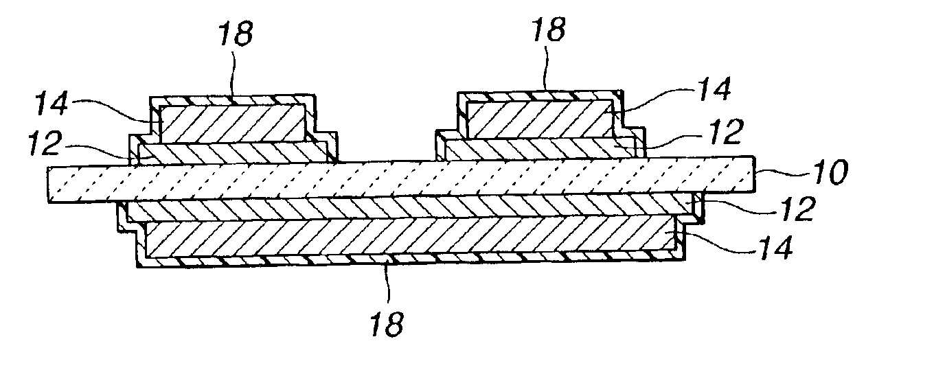
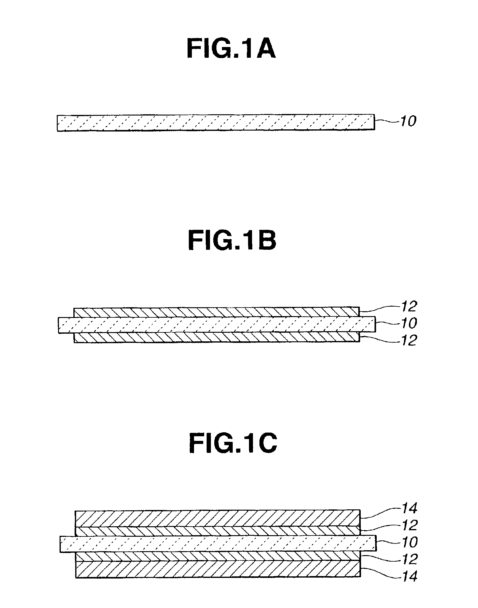
[0052]Then, as shown in FIGS. 1A through 1C, a ceramic substrate 10 was prepared (FIG. 1A), and the brazing filler metal 12 was applied on both sides of the ceramic substrate 10 by the screen printing (FIG. 1B). Then, copper plates 14 having a thickness of 0.3 mm were arranged on both sides thereof, and the copper plates 14 were bonded to the ceramic substrate 10 at 835° C. in a vacuum furnace. In order to verify the thickness of the brazing filler metal 12, the sample thus bonded was cut to measure the thickness of the brazing filler metal 12. As a result, the thickness of the brazing filler metal 12 was about 20 μm. As the ceramic substrate 10, an S g...

example 2

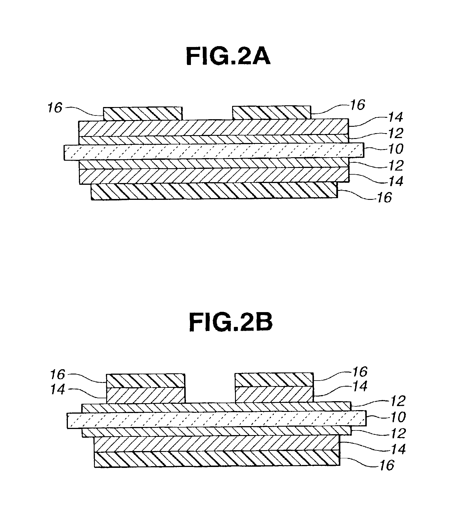
[0056]The substrate treated with the mixed solution of EDTA, aqueous hydrogen peroxide and pH regulator in Example 1 was treated with an etchant comprising copper chloride, hydrochloric acid and hydrogen peroxide again. Then, the resists were peeled off, and the Ni—P electroless plating was carried out. The brazing filler metal protruding length of the metal / ceramic bonding circuit board obtained in this example was 120 μm, and the brazing filler metal removing performance and circuit pattern performance thereof were good.

example 3

[0057]The same treatment as that in Example 2 was carried out, except that Al2O3 was used as the ceramic. The brazing filler metal protruding length of the metal / ceramic bonding circuit board obtained in this example was 120 μm, and the brazing filler metal removing performance and circuit pattern performance thereof were good.


PUM

PropertyMeasurementUnit
pHaaaaaaaaaa
lengthaaaaaaaaaa
thicknessaaaaaaaaaa

Abstract

After copper plates 14 are bonded to both sides of a ceramic substrate 10 via a brazing filler metal 12, UV curing alkali peeling type resists 16 are applied on predetermined portions of the surfaces of the copper plates 14 to etch undesired portions of the copper plates 14 to form a metal circuit portion. While the resists 16 are maintained, undesired portions of the brazing filler metal 12 and a reaction product, which is produced by a reaction of the brazing filler metal 12 with the ceramic substrate 10, are removed (or undesired portions of the brazing filler metal 12 and a reaction product, which is produced by a reaction of the brazing filler metal 12 with the ceramic substrate 10, are removed, and the side portion of the metal circuit portion is etched). Thereafter, the resists 16 are peeled off, and an Ni—P electroless plating 18 is carried out. Thus, in a method for producing a metal / ceramic bonding circuit board, it is possible to easily control the sectional shape of a metal / ceramic bonding circuit board by a smaller number of steps and at low costs, and it is possible to produce a metal / ceramic bonding circuit board which is more reliable with respect to thermal shock resistance and insulation performance.

Description

BACKGROUND OF THE INVENTION[0001]1. Field of the Invention[0002]The present invention generally relates to a method for producing a metal / ceramic bonding circuit board. More specifically, the invention relates to a method for producing a metal / ceramic bonding circuit board wherein a metal plate is bonded to a ceramic substrate via a brazing filler metal to form a circuit and on which a large power element, such as a power module, is suitably mounted.[0003]2. Description of the Prior Art[0004]In a typical method for producing a ceramic circuit board for a power module or for mounting a semiconductor thereon, a metal plate and a ceramic substrate are first bonded to each other. For example, there is industrially utilized the direct bonding method for arranging a copper plate on a ceramic substrate so as to allow the copper plate to directly contact the ceramic substrate and for heating the copper plate and the ceramic substrate in an inert gas to bond the ceramic substrate and the cop...

Claims


Application Information

Patent Timeline
Patent Type & Authority Patents(United States)
IPC IPC(8): H05K3/26H05K3/06H05K3/38H05K1/03B23K1/00B23K1/19C04B37/02H05K3/24
CPCH05K3/06H05K3/26H05K3/38H05K1/0306H05K3/064H05K2201/0355H05K2201/0761H05K2203/0796H05K2203/1184H05K2203/121
Inventor TSUKAGUCHI, NOBUYOSHIKIMURA, MASAMI
Owner DOWA METALS & MINING CO LTD
Why Eureka
Try Eureka