Thin channel FET with recessed source/drains and extensions

a thin channel, source/drain technology, applied in the field of high-performance field-effect transistors (fets), can solve the problems of device leakage including gate leakage, chip power consumption has increased, and cooling and packaging costs have increased, so as to improve ultra-thin soi performance, reduce external resistance of ultra-thin soi devices, and improve the effect of ultra-thin soi performan

Inactive Publication Date: 2005-08-02
IBM CORP
View PDF25 Cites 24 Cited by
  • Summary
  • Abstract
  • Description
  • Claims
  • Application Information

AI Technical Summary

Benefits of technology

[0011]It is a purpose of the invention to improve ultra-thin SOI performance;
[0012]It is another purpose of the invention to reduce ultra-thin SOI device external resistance;
[0013]It is yet another purpose of the invention to reduce external resistance in ultra-thin SOI devices without increasing device parasitic capacitance.

Problems solved by technology

Thus, not withstanding the decrease of chip supply voltage, chip power consumption has increased as well.
Both at the chip and system levels, cooling and packaging costs have escalated as a natural result of this increase in chip power.
Unfortunately, as FET features have shrunk, device leakages including gate leakages (i.e., gate to channel, gate to source or drain and gate induced drain leakage (GIDL)) and source / drain junction leakages have become pronounced.
This resulted in a buried leakage path between the source / drain regions and, in some cases in sub-surface channel shorts.
Unfortunately, these lightly doped regions add series resistance at the source and drain of each device, which reduces device currents and degrades circuit performance.
Furthermore, as device channel lengths have shrunk well below one micron (1 μm), subthreshold problems have become more pronounced and lightly doped drains does not solve those problems.
Unfortunately, however, because source / drain regions are made from the same ultra-thin SOI layer, devices have higher external resistance.
Unfortunately, raised source / drains above the silicon layer surface places parallel surface areas at each side of the gate, requiring gaps at gate sidewalls (e.g., spacers) to prevent shorts and, simultaneously causing increased parasitic gate capacitance between the gate and the RSD regions.
Unfortunately, both Xiang et al. tolerates resistive extensions that connect the device channel to the recessed source / drain regions and that function similarly to LDD, adding series source / drain resistance.
Thus, previously, one was faced with accepting parasitic device capacitances, series channel resistances and / or looser design tolerances.

Method used


Image

  • Thin channel FET with recessed source/drains and extensions
  • Thin channel FET with recessed source/drains and extensions
  • Thin channel FET with recessed source/drains and extensions

Examples


Embodiment Construction

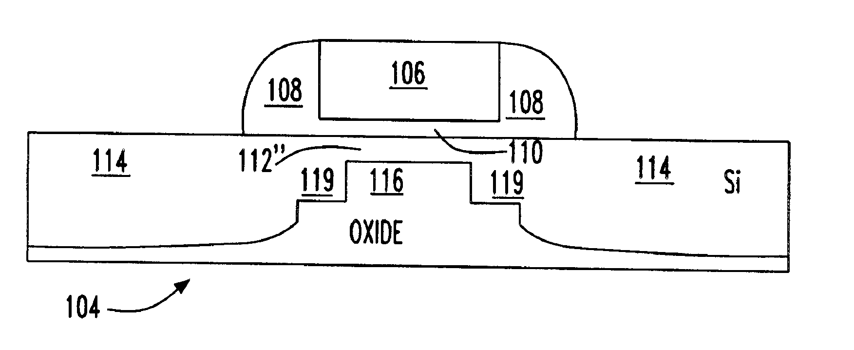
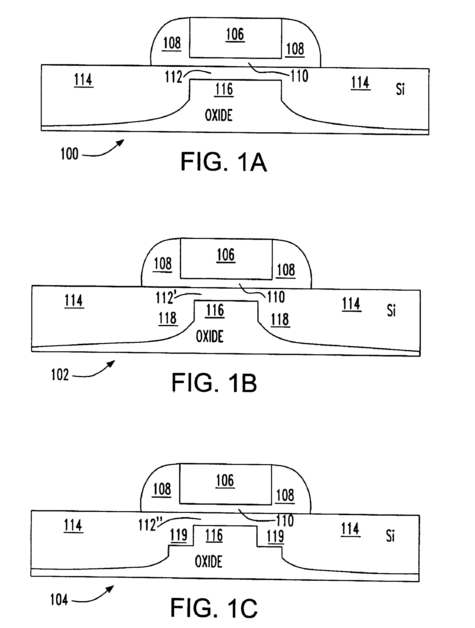
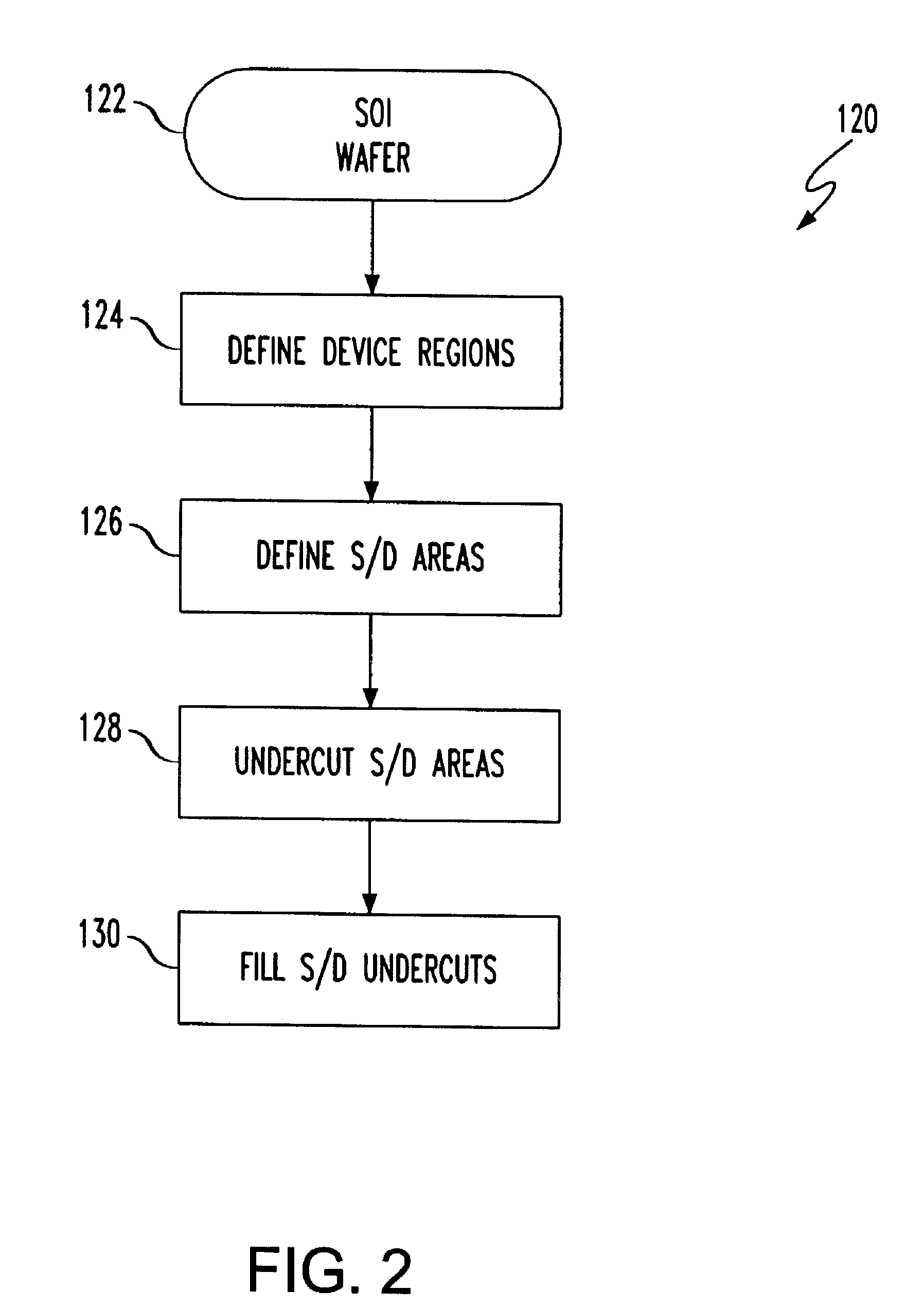
[0024]Turning now to the drawings and, more particularly, FIGS. 1A-C, each show an example of a field effect transistor (FET) 100, 102, 104 with self aligned recessed source / drain regions and extensions according to a preferred embodiment of the present invention with like elements labeled identically. In particular, FETs 100, 102, 104 may be typical devices in a circuit, such as a CMOS circuit on an ultra-thin (smaller than or equal to 15 nanometers (10 nm)) semiconductor on insulator (SOI) CMOS chip.

[0025]So, in the FET 100 example of FIG. 1A, a gate 106 has spacers 108 at each side. Preferably, the gate 106 is polysilicon, a metal, silicon-germanium (SiGe), a silicide or combination thereof and the spacers 108 are nitride. The gate 106 is on a gate dielectric layer 110 (e.g., oxide) above an ultra-thin channel 112, an ultra-thin semiconductor layer of strained silicon (SSi), Germanium (Ge), SiGe or, preferably, silicon (Si). The ultra-thin channel 112 is less than 40 nm long and,...


PUM


Abstract

A field effect transistor (FET), integrated circuit (IC) chip including the FETs and a method of forming the FETS. The devices have a thin channel, e.g., an ultra-thin (smaller than or equal to 10 nanometers (10 nm)) silicon on insulator (SOI) layer. Source / drain regions are located in recesses at either end of the thin channel and are substantially thicker (e.g., 30 nm) than the thin channel. Source / drain extensions and corresponding source / drain regions are self aligned to the FET gate and thin channel.

Description

BACKGROUND OF INVENTION[0001]The present invention is related to semiconductor devices and manufacturing and more particularly to high performance field effect transistors (FETS) and methods of manufacturing high performance FETS.[0002]Typical semiconductor integrated circuit (IC) design goals include high performance and density at minimum power. To minimize semiconductor circuit power consumption, most ICs are made in the well-known complementary insulated gate field effect transistor (FET) technology known as CMOS. A typical CMOS circuit drives a purely or nearly pure capacitive load and includes paired complementary devices, i.e., an n-type FET (NFET) paired with a corresponding p-type FET (PFET), usually gated by the same signal. Performance depends upon how fast the CMOS circuit can charge and discharge the capacitive load, i.e., the circuit's switching speed. Since the pair of devices have operating characteristics that are, essentially, opposite each other, when one device (...

Claims


Application Information

Patent Timeline
Patent Type & Authority Patents(United States)
IPC IPC(8): H01L21/336H01L29/786H01L29/10H01L29/02H01L21/02H01L29/66
CPCH01L29/1054H01L29/66772H01L29/78603H01L29/78618H01L29/78621H01L29/78696H01L29/78684
Inventor CHEN, HUAJIEDORIS, BRUCE B.OLDIGES, PHILIP J.WANG, XINLINZHU, HUILONG
Owner IBM CORP
Why Eureka
Try Eureka