Apparatus for reshaping a patterned organic photoresist surface

Inactive Publication Date: 2005-08-16
APPLIED MATERIALS INC
View PDF45 Cites 7 Cited by
  • Summary
  • Abstract
  • Description
  • Claims
  • Application Information

AI Technical Summary

Benefits of technology

[0015]It is difficult to do the metrology which indicates whether a patterned photoresist will provide a desired reticle critical dimension when a foot is present at the base of the patterned photoresist. The metrology is particularly inaccurate since the size of the foot typically varies at different locations across the reticle fabrication structure. Metrology may be carried out after patterning of the photoresist or may be carried out after the pattern has been transferred through the chrome-containing masking layer. The significant cost of transferring a defective pattern from a patterned photoresist through several underlying layers to form the reticle can be avoided by conducting metrology for the

Problems solved by technology

It is difficult to do the metrology which indicates whether a patterned photoresist will provide a

Method used


Image

  • Apparatus for reshaping a patterned organic photoresist surface
  • Apparatus for reshaping a patterned organic photoresist surface
  • Apparatus for reshaping a patterned organic photoresist surface

Examples


example one

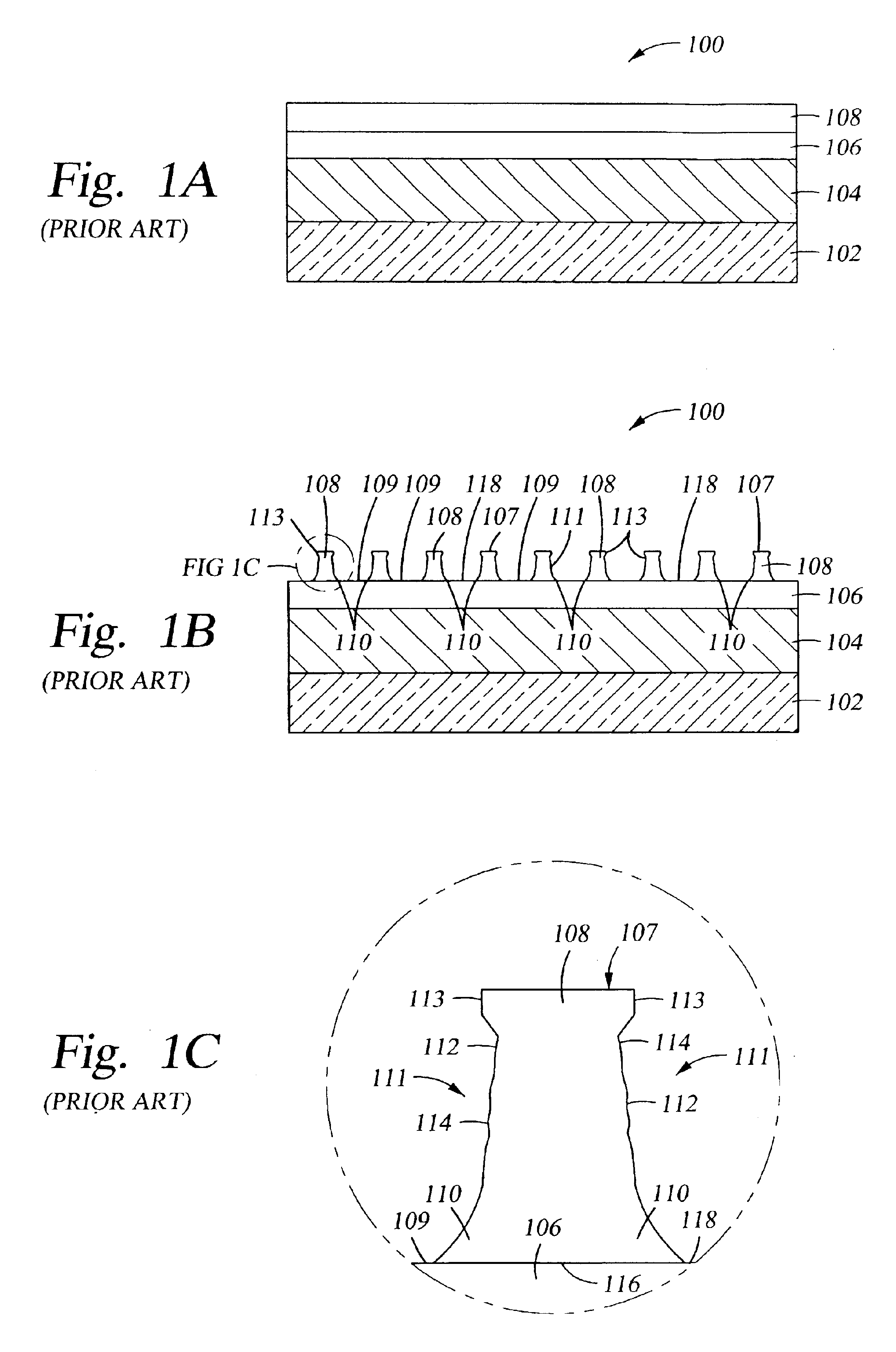
[0037]FIG. 1A shows a typical starting structure 100 used in the fabrication of a photomask, hereafter referred to as a reticle. In this Example, starting structure 110 was a stack of layers which included, from top to bottom, a 5,000 Å thick layer of a chemically amplified DUV photoresist, DX1100 (available from AZ Clariant Corp. of Somerville, N.J.); a 250 Å thick layer of an inorganic ARC, chrome oxynitride; a 750 Å thick layer of a mask material which is essentially chrome; and a silicon oxide-containing substrate.

[0038]In particular, the chemically amplified DUV photoresist comprises propylene glycol monomethyl; ether acetate; PMA; PGMEA; 1-methoxy-2-propyl acetate; modified phenolic polymer; and an onium salt metal halide complex as a chemical amplifier. The inorganic ARC was CrOxNy. The chrome-containing mask material was essentially chrome. The silicon oxide-containing substrate was quartz.

[0039]FIG. 1B shows a schematic cross-sectional view of the patterned photoresist laye...

example two

[0046]FIG. 3A shows a schematic of an isolated contact pad structure taken from a photomicrograph of a patterned photoresist layer 328, where the photoresist layer 328 was patterned in the manner described with reference to Example One, above. In this Example, the starting reticle structure was the same as described above; a stack of layers which included, from top to bottom, a 5,000 Å thick layer of DUV photoresist DX1100; a 250 Å thick layer of a CrOxNyARC; a 750 Å thick layer of chrome masking material; and a quartz substrate. The contact pad was essentially square, having a 0.75 μm length pad. Even after descumming, the presence of standing waves 324 on the surface 322 of sidewalls 327 was evident. In addition, a substantial foot 330 was present at the base of sidewalls 327 where photoresist 328 contacted ARC layer 326.

[0047]Again, we discovered it was possible to reshape the surface 322 of the patterned photoresist 328 to remove standing waves 324 and foot 330 by exposing the s...

example three

[0048]The range of process conditions useful in the reshaping of a patterned photoresist surface using an oxygen-comprising plasma are as follows, for a chemically amplified DUV photoresist comprising at least one ether acetate, and a modified phenolic polymer:

[0049]

TABLE IGeneral RangePreferred RangeMost PreferredProcess Variableof Variableof VariableRange of VariablePlasma Source10-20010-5015-19Gas Flow Rate(O2 sccm)*Process Chamber1-50 3-203-7Pressure (mTorr)RF Power to 1-500100-200120-130Cathode (W) at13.56 MHz**Substrate Bias10-750200-500350-400(- V)Substrate5-5010-3012-25Temperature(° C.)Process Chamber25-90 30-6035-50Temperature ° C.Processing Time15-24030-9050-70(sec)*An inert diluent gas such as a noble gas (He, Ar, Kr, Ne, Xe) may be used in combination with the O2, where the total gas flow remains the same as that specified. **It is contemplated that other power frequencies may be used.

[0050]One skilled in the art will recognize that the process conditions provided in Ta...


PUM

PropertyMeasurementUnit
Dimensionaaaaaaaaaa
Antireflectiveaaaaaaaaaa

Abstract

The invention relates to a method of improving control over the dimensions of a patterned photoresist, which enables better control of the critical dimensions of a photomask or reticle which is fabricated using the patterned photoresist. In addition, the method may be used to enable improved control over the dimensions of a semiconductor device fabricated using a patterned photoresist. In particular, a patterned photoresist is treated with an etchant plasma to reshape the surface of the patterned photoresist, where reshaping includes the removal of “t”-topping at the upper surface of the patterned resist, the removal of standing waves present on patterned surfaces, and the removal of feet which may be present at the base of the patterned photoresist, where the photoresist contacts an underlying layer such as an ARC layer. The method is particularly useful for chemically amplified DUV photoresists, where the presence of “t”-topping, standing waves and foot formation is accentuated in the patterned photoresist as developed.

Description

[0001]This application is a divisional application of application Ser. No. 09 / 811,186, filed Mar. 16, 2001, now U.S. Pat. No. 6,582,861.BACKGROUND OF THE INVENTION[0002]1. Field of the Invention[0003]In general, the present invention relates to a method of reshaping a patterned photoresist. The surface of the patterned photoresist material is “trimmed” and “refinished”, to improve the pattern profile and surface finish of the patterned photoresist. The method is particularly useful in the preparation of reticles which are used in combination with an exposure tool to image photoresist layers overlying a semiconductor substrate. The method may also be used to prepare a photoresist masking layer which is used to transfer a pattern to an underlying hard masking material on a semiconductor substrate. The method is useful for reshaping patterned i-line photoresists and is particularly beneficial when the patterned photoresist is a deep ultra violet (DUV) photoresist.[0004]2. Brief Descrip...

Claims


Application Information

Patent Timeline
IPC IPC(8): G03F7/40G03F7/09G03F7/00G03F9/00
CPCG03F7/40G03F7/091
Inventor BUXBAUM, ALEXMONTGOMERY, MELVIN W.
Owner APPLIED MATERIALS INC
Why Eureka
Try Eureka