

Semiconductor capacitor with diffusion prevention layer
a technology of diffusion prevention layer and capacitor, which is applied in the direction of resistors, basic electric elements, solid-state devices, etc., can solve the problems of increased leakage current of capacitors, loss of contact between the etc., and achieve high-performance capacitors, desired electric characteristics, and improved electrical connection between the conductive plug and the lower electrode
- Summary
- Abstract
- Description
- Claims
- Application Information
AI Technical Summary
Benefits of technology
Problems solved by technology
Method used
Image

Examples
first embodiment
[0047](First Embodiment)
[0048]A semiconductor device having a capacitor according to a first embodiment of the present invention and a method of manufacturing the same will be explained with reference to FIG. 1 to FIG. 7 hereunder.
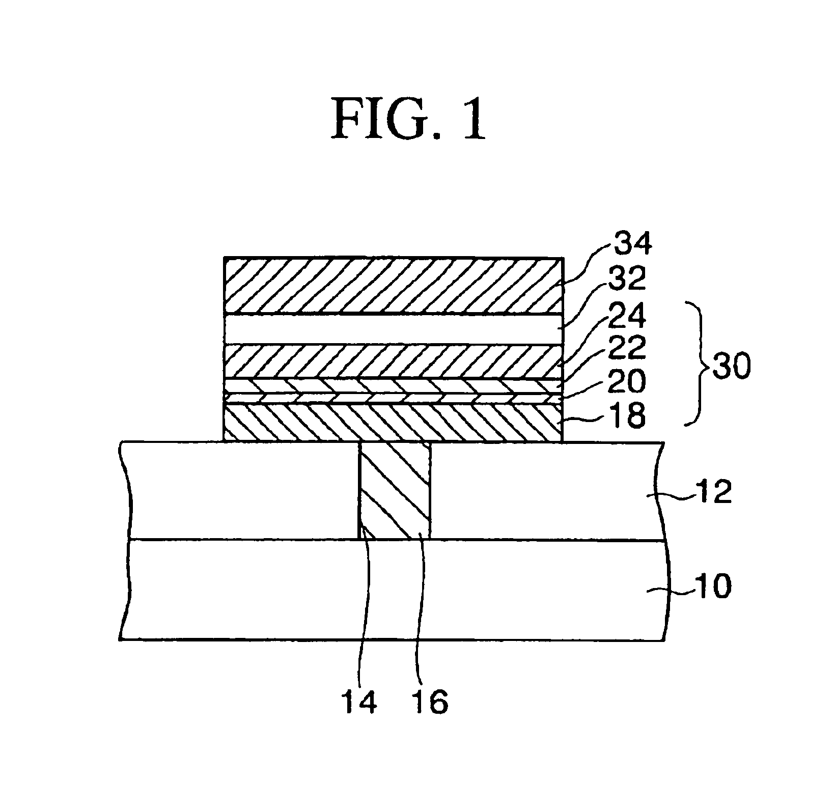
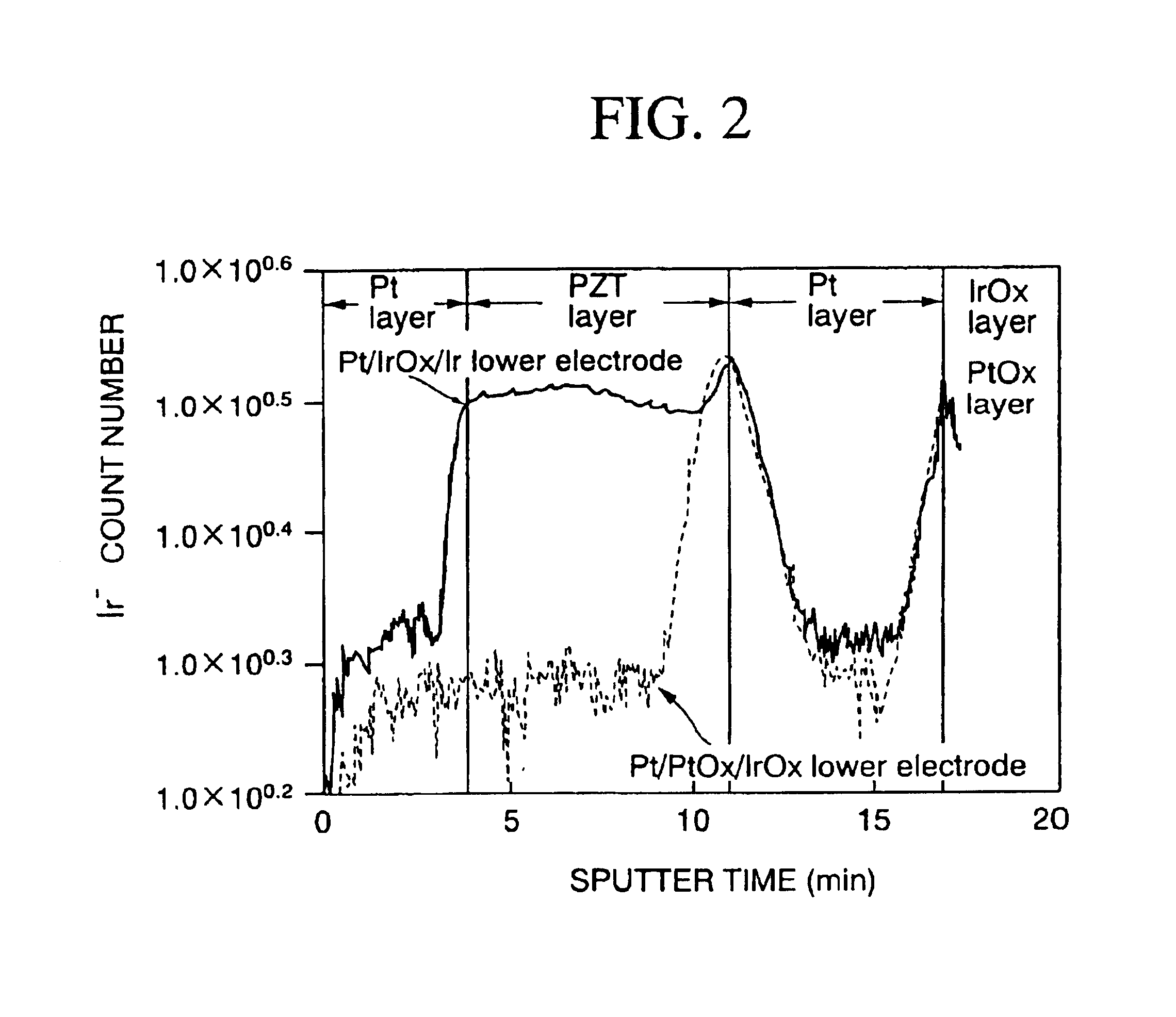
[0049]FIG. 1 is a schematic sectional view showing a structure of a capacitor according to a first embodiment. FIG. 2 is a graph showing the diffusion of iridium in the capacitor and the diffusion preventing effect. FIGS. 3A to 3C are sectional views showing steps in a method of manufacturing the capacitor according to the first embodiment. FIG. 4 is a graph showing the dependency of the residual electric charge amount on the substrate temperature in the capacitor according to the first embodiment. FIG. 5 is a graph showing the dependency of the leakage current on the substrate temperature in the capacitor according to the first embodiment. FIG. 6 is a graph showing the dependency of the residual electric charge amount on the gas flow rate ratio in the cap...
second embodiment
[0086](Second Embodiment)
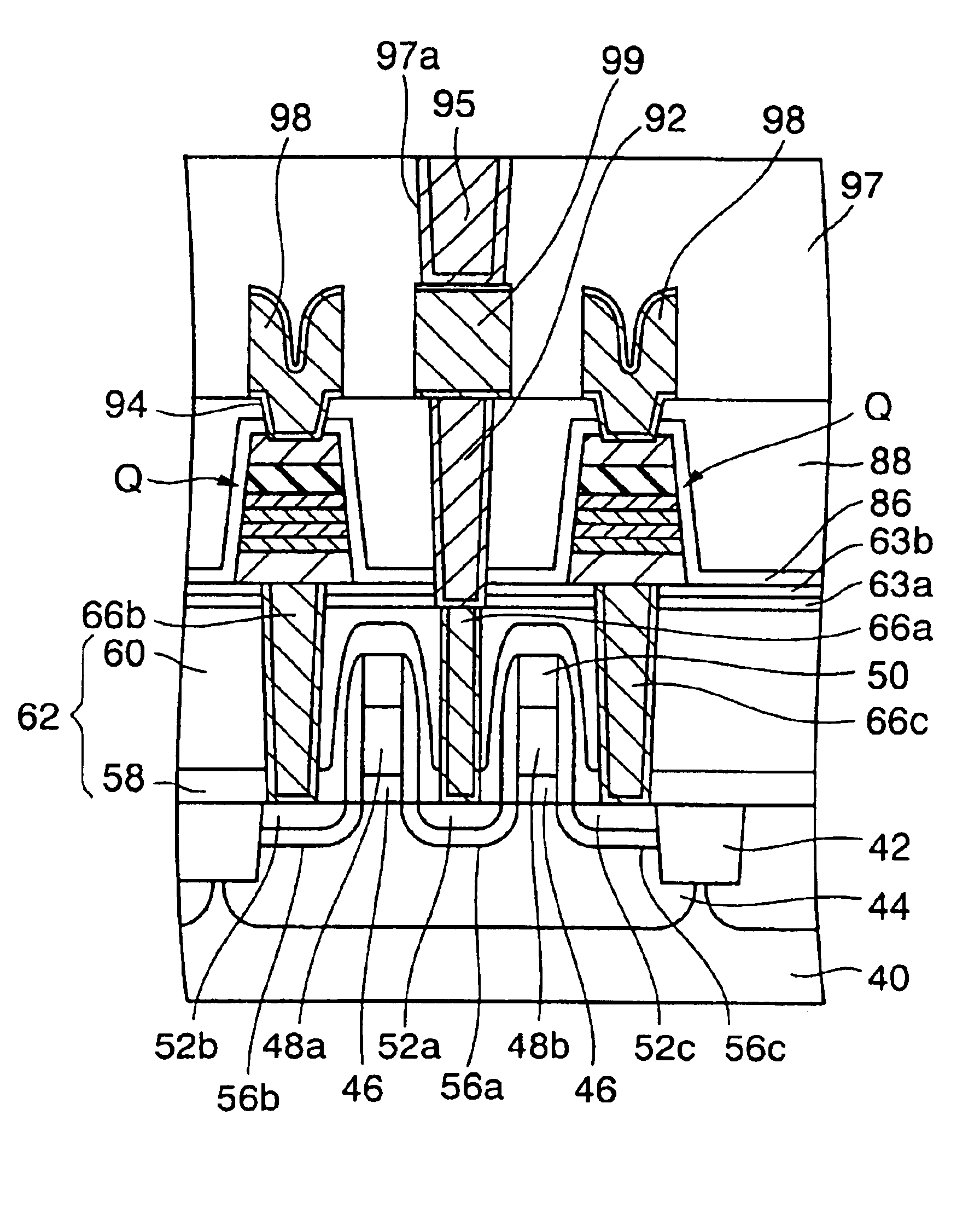
[0087]A semiconductor device and a method of manufacturing the same according to a second embodiment of the present invention will be explained with reference to FIG. 8 to FIGS. 11A to 11C hereunder.
[0088]FIG. 8 is a schematic sectional view showing a structure of a semiconductor device according to a second embodiment. FIGS. 9A to 9D, FIGS. 10A to 11C, and FIGS. 11A to 11C are sectional views showing steps in a method of manufacturing the semiconductor device according to the second embodiment.
[0089]First of all, the structure of the semiconductor device according to the second embodiment will be explained with reference to FIG. 8 hereunder.
[0090]An element isolation layer 42 is formed on a silicon substrate 40. Memory cell transistors having gate electrodes 48 and source / drain diffusion layers 56 are formed in an element region that is defined by the element isolation layer 42. An interlayer insulating layer 62 is formed on the silicon substrate 40 on whic...
third embodiment
[0127](Third Embodiment)
[0128]The present invention is not limited to the above embodiments and various variations may be applied.
[0129]For example, in the above embodiments, the IrOx / Ir structure and the Ir single-layer structure are shown as the oxygen diffusion barrier layer. In order to prevent the diffusion of the oxygen, at least the IrOx layer or the Ir layer may be formed between the plug and the capacitor dielectric layer. Therefore, other conductive layer in addition to the Ir / IrOx structure, the IrOx layer, the Ir layer, or the like may be formed. In this case, if the orientation control of the capacitor dielectric layer is taken into consideration, it is desired that, as described above, the uppermost layer should be formed of IrOx.
[0130]Also, in the above embodiments, the platinum oxide layer is employed as the iridium diffusion barrier layer, but such platinum oxide layer may be employed by other conductive layer. There are the platinum group elements as the element ha...
PUM
| Property | Measurement | Unit |
|---|---|---|
| temperature | aaaaa | aaaaa |
| temperature | aaaaa | aaaaa |
| applied voltage | aaaaa | aaaaa |
Abstract
Description
Claims
Application Information