Method of manufacturing a semiconductor device and manufacturing system thereof

a manufacturing system and semiconductor technology, applied in the direction of semiconductor devices, electrical devices, transistors, etc., can solve the problems of lowering the general purpose of the liquid crystal panel, reducing the degree of productivity and reliability, and complicated wiring structure, so as to promote the elimination of hydrogen, constant processing effect, and high reproducibility

Inactive Publication Date: 2005-08-23
SEMICON ENERGY LAB CO LTD
View PDF76 Cites 8 Cited by
  • Summary
  • Abstract
  • Description
  • Claims
  • Application Information

AI Technical Summary

Benefits of technology

[0059]As a silicon film which is subjected to the plasma processing, the use of amorphous silicon can obtain the highest effect. This is because hydrogen of 20 to 30 atms % is contained in the amorphous silicon film.
[0210]Further, a processing chamber in which the elimination of hydrogen from the amorphous silicon film is promoted, and a processing chamber in which the silicon film from which the elimination of hydrogen has been promoted is crystallized are coupled to a transportation chamber for transporting a substrate, and the above processing and the transportation of the substrate are conducted in a state where it is isolated from the external, thereby being capable of obtaining constant processing effects with respect to a plurality of substrates. In other words, the crystalline silicon film which is uniform in crystalline property for each substrate can be obtained. Further, a high productivity can be obtained.

Problems solved by technology

However, this structure is complicated in wiring from the IC chip and lower in productivity and reliability.
This problem leads to the lowering of the degree of the general purpose of the liquid-crystal panel.
However, those devices lead to such a situation that the operation method or the circuit structure is complicated, to thereby lower the practicability.
However, in case of using a thin-film transistor in the active matrix liquid-crystal electro-optic device, there arises such a problem that a glass substrate need be utilized as a substrate from the viewpoint of economics.
However, even though a thin-film transistor is constituted using the crystalline silicon film obtained in the above manner, the transistor cannot operate at a frequency except for several MHz or lower.
However, the quartz substrate or the specified glass substrate that withstands a high temperature is expensive and therefore difficult to use from the viewpoint of the production costs.
In case of utilizing the irradiation of a laser beam, a crystalline silicon film which is partially very excellent in crystalline property can be obtained, whereas there arise such problems that it is hard to obtain the uniformity of the effect of irradiation of a laser beam over the entire film, and also that even the crystalline silicon films as obtained are increased in dispersion every process (in other words, low in reproducibility).

Method used


Image

  • Method of manufacturing a semiconductor device and manufacturing system thereof
  • Method of manufacturing a semiconductor device and manufacturing system thereof
  • Method of manufacturing a semiconductor device and manufacturing system thereof

Examples


first embodiment

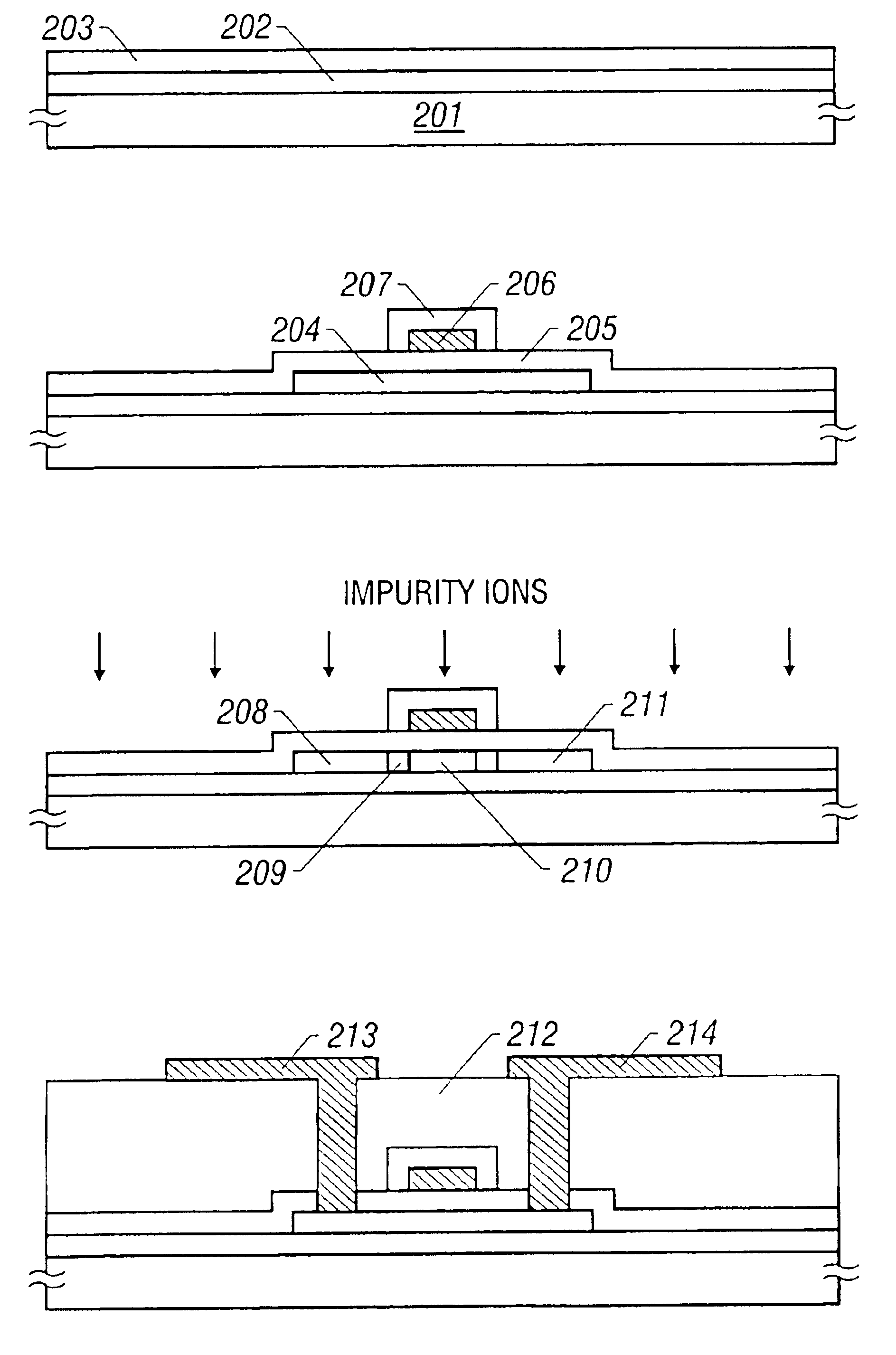
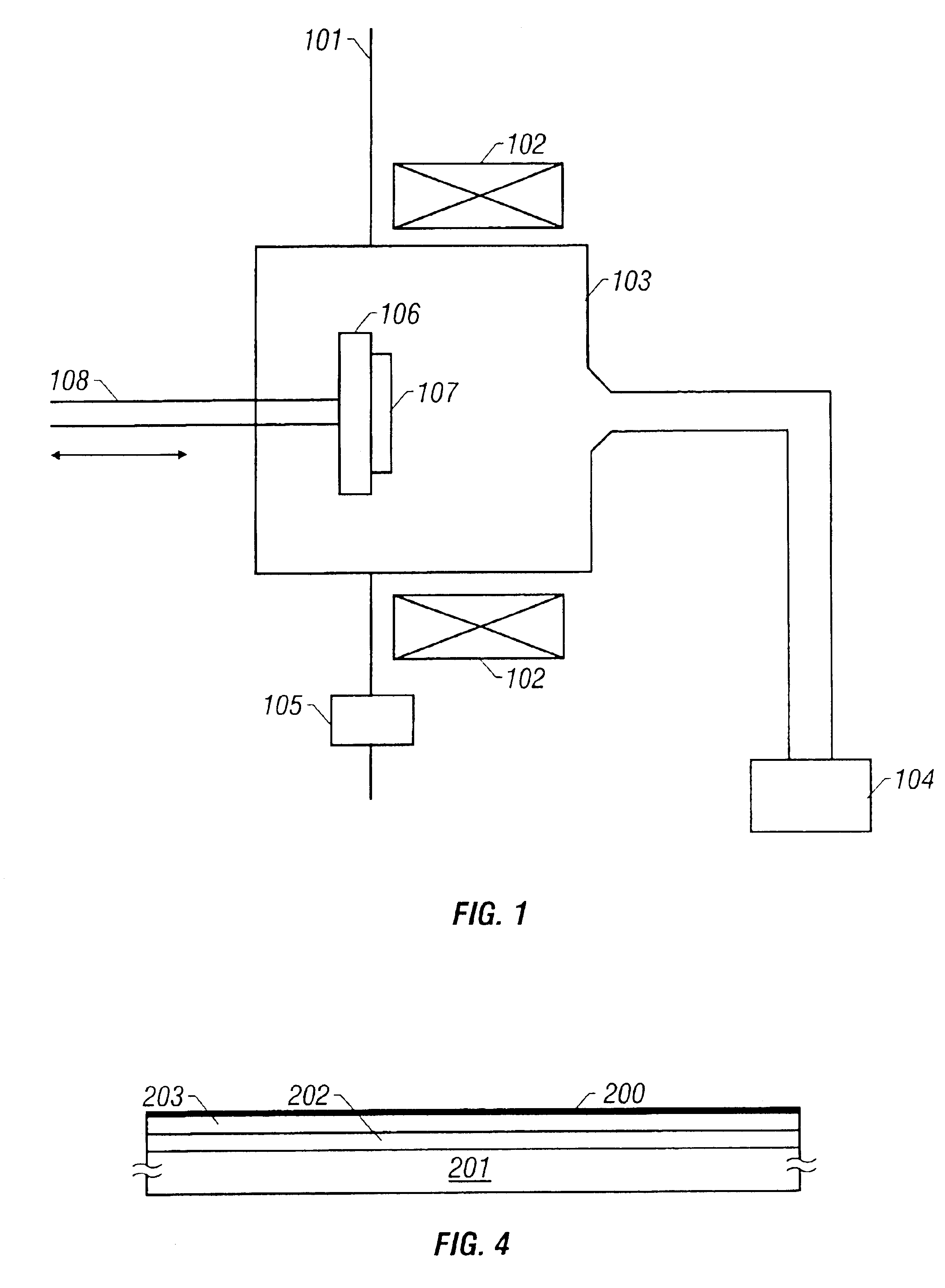
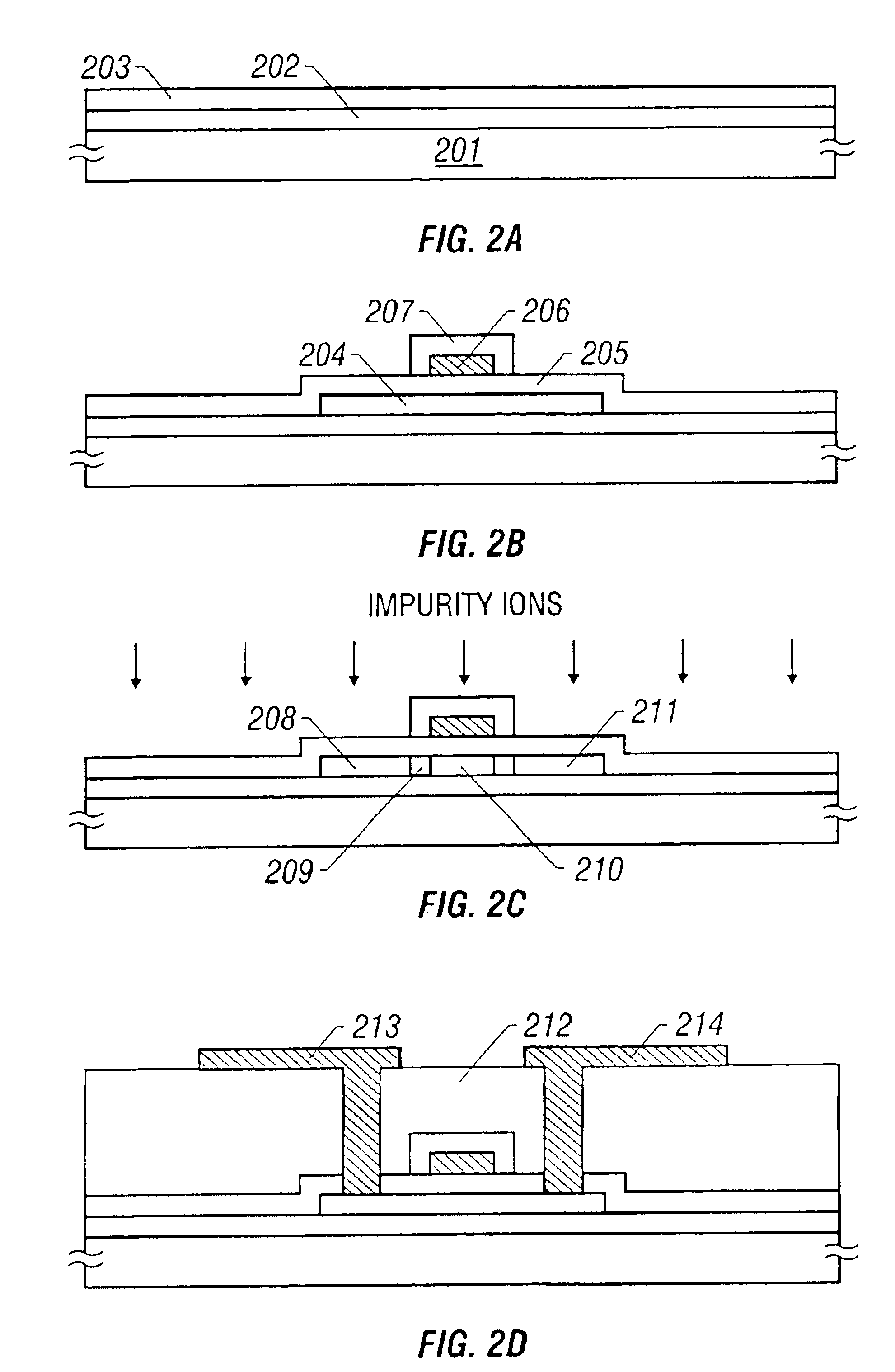
[0231]A first embodiment relates to a structure in which a crystalline silicon film is formed on a glass substrate. First, a silicon oxide film is formed on a glass substrate as an under layer. The silicon oxide film functions to relieve the diffusion of impurities in the glass substrate and a stress produced between the glass substrate and a semiconductor film. The silicon oxide film may be formed at a thickness of about 3000 Å through the plasma CVD technique or the sputtering technique.

[0232]Then, an amorphous silicon film is formed on the silicon oxide film. The amorphous silicon film may be formed through the plasma CVD technique or the decompression thermal CVD technique. The thickness of the amorphous silicon film may be set to a required value, but is set to 500 Å in this embodiment.

[0233]After the formation of the amorphous silicon film, a hydrogen plasma is produced under decompression through a technique using a magnetic field and a microwave, and the above-mentioned amor...

second embodiment

[0240]A second embodiment relates to a structure in which a crystalline silicon film is formed on a glass substrate, using the catalysis of a metal element. First, a silicon oxide film is formed on a glass substrate as an under layer. The silicon oxide film functions to relieve the diffusion of impurities in the glass substrate and a stress produced between the glass substrate and a semiconductor film. The silicon oxide film may be formed at a thickness of about 3000 Å through the plasma CVD technique or the sputtering technique.

[0241]Then, an amorphous silicon film is formed on the silicon oxide film. The amorphous silicon film may be formed through the plasma CVD technique or the decompression thermal CVD technique. The thickness of the amorphous silicon film may be set to a required value, but is set to 500 Å in this embodiment.

[0242]After the formation of the amorphous silicon film, metal elements that promote the crystallization of silicon is held in contact with the surface of...

third embodiment

[0252]A third embodiment relates to a structure in which the order of a process of introducing the metal elements that promote the crystallization of silicon and a process of the plasma processing are reversed in the processes described in the second embodiment. In other words, a plasma processing is conducted after the formation of the amorphous silicon film, and thereafter a plasma processing is conducted on the silicon film which has been plasma processing. With those processes, the inside of a chamber for conducting the plasma processing can be prevented from being contaminated by the metal elements.


PUM

PropertyMeasurementUnit
temperatureaaaaaaaaaa

Abstract

A method of manufacturing a semiconductor device, comprises the steps of: forming an amorphous silicon film on a substrate having an insulating surface; processing said amorphous silicon film by plasma of a gas that mainly contains hydrogen or helium; and giving an energy to said amorphous silicon film.

Description

[0001]This is a divisional of U.S. application Ser. No. 08 / 616,623, filed Mar. 15, 1996 now U.S. Pat. No. 5,956,581.BACKGROUND OF THE INVENTION[0002]1. Field of the Invention[0003]The present invention relates to a method of manufacturing a thin-film semiconductor device which is formed on a substrate having an insulating surface of a glass substrate or the like. Also, the present invention relates to a method of manufacturing a semiconductor device (for example, a thin-film transistor) using a thin-film semiconductor device.[0004]2. Description of the Related Art[0005]In recent years, attention has been paid to a thin-film transistor as a semiconductor device using a thin-film semiconductor device. In particular, attention has been paid to a structure in which a thin-film transistor is mounted on a liquid-crystal electro-optic device. This is to constitute the thin-film transistor using a thin-film semiconductor device which is formed on a glass substrate constituting the liquid-cr...

Claims


Application Information

Patent Timeline
Patent Type & Authority Patents(United States)
IPC IPC(8): H01L21/02H01L21/70H01L21/30H01L21/84H01L21/336H01L21/20H01L21/00H01L21/77H01L27/12H01L29/786
CPCH01L21/3003H01L27/12H01L29/66757H01L29/78675H01L27/1277H01L21/2026H01L21/67155H01L29/66765H01L21/02686H01L21/02532H01L21/02672H01L21/02422H01L21/02488
Inventor YAMAZAKI, SHUNPEITERAMOTO, SATOSHIKUSUMOTO, NAOTOOHNUMA, HIDETO
Owner SEMICON ENERGY LAB CO LTD
Why Eureka
Try Eureka