Zinc oxide semiconductor material

a technology of zinc oxide and semiconductor material, applied in the direction of non-metal conductors, conductors, crystal growth processes, etc., can solve the problems of difficult to obtain a single crystal film of relatively large area, luminous light characteristic, doping characteristic deterioration, etc., to achieve easy and inexpensive availability of raw materials, reduce the quantity of carbon in the resulting zinc oxide semiconductor material, and reduce the effect of luminous light characteristi

Inactive Publication Date: 2005-08-30
TOHOKU TECHNO ARCH CO LTD +1
View PDF11 Cites 18 Cited by
  • Summary
  • Abstract
  • Description
  • Claims
  • Application Information

AI Technical Summary

Benefits of technology

[0007]Whereas a c-axial orientation plane having a hexagonal crystal plane is apt to form nanocrystals by minimizing the hexagonal shape when the shape is even slightly deformed, the a-axial crystal orientation plane oriented to the a-axis of the wurtzite structure hardly forms the nanocrystals as described above because it has a rectangular shape capable of moderating a slight strain, so that stable crystals of high quality similar to single crystal can be provided in a wide area, and the deterioration of doping characteristic, luminous characteristic and the like can be consequently prevented. The a-axial plane is also more excellent in doping characteristic than the c-axial plane, allowing the stable preparation of a semiconductor.
[0011]According to this, the MO-CVD method in which an inexpensive device was usable but it was difficult to obtain a crystal of high quality can be used to prepare a zinc oxide semiconductor material at a low cost.
[0013]By using the zinc acetylacetonate (Zn(acac)2), not only the carbon quantity in the resulting zinc oxide semiconductor material can be minimized, but also the raw material is easily and inexpensively available because the zinc acetylacetonate is industrially produced in large quantities.

Problems solved by technology

However, not only such a crystal having c-axial orientation is apt to form a polycrystal containing nanocrystals, when the shape is even slightly deformed in the growing stage of crystal, by minimizing the hexagonal shape to arrest the deformation, which makes it difficult to obtain a single crystal film of relatively large area, but also a polycrystal film containing the nanocrystals is apt to cause abnormal properties in electric conduction by the bonding of impurities to the terminal of the nanocrystals or the bonding of a conductive electron to a dangling bond at the top surface, resulting in the deterioration of doping characteristic, luminous light characteristic, and the like.

Method used


Image

  • Zinc oxide semiconductor material
  • Zinc oxide semiconductor material
  • Zinc oxide semiconductor material

Examples


example

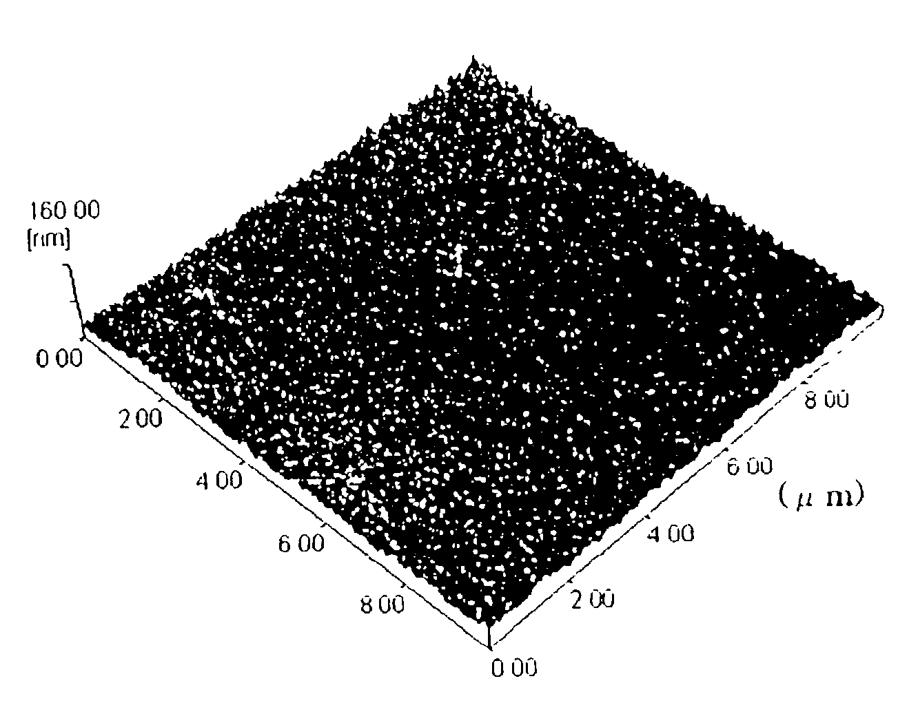
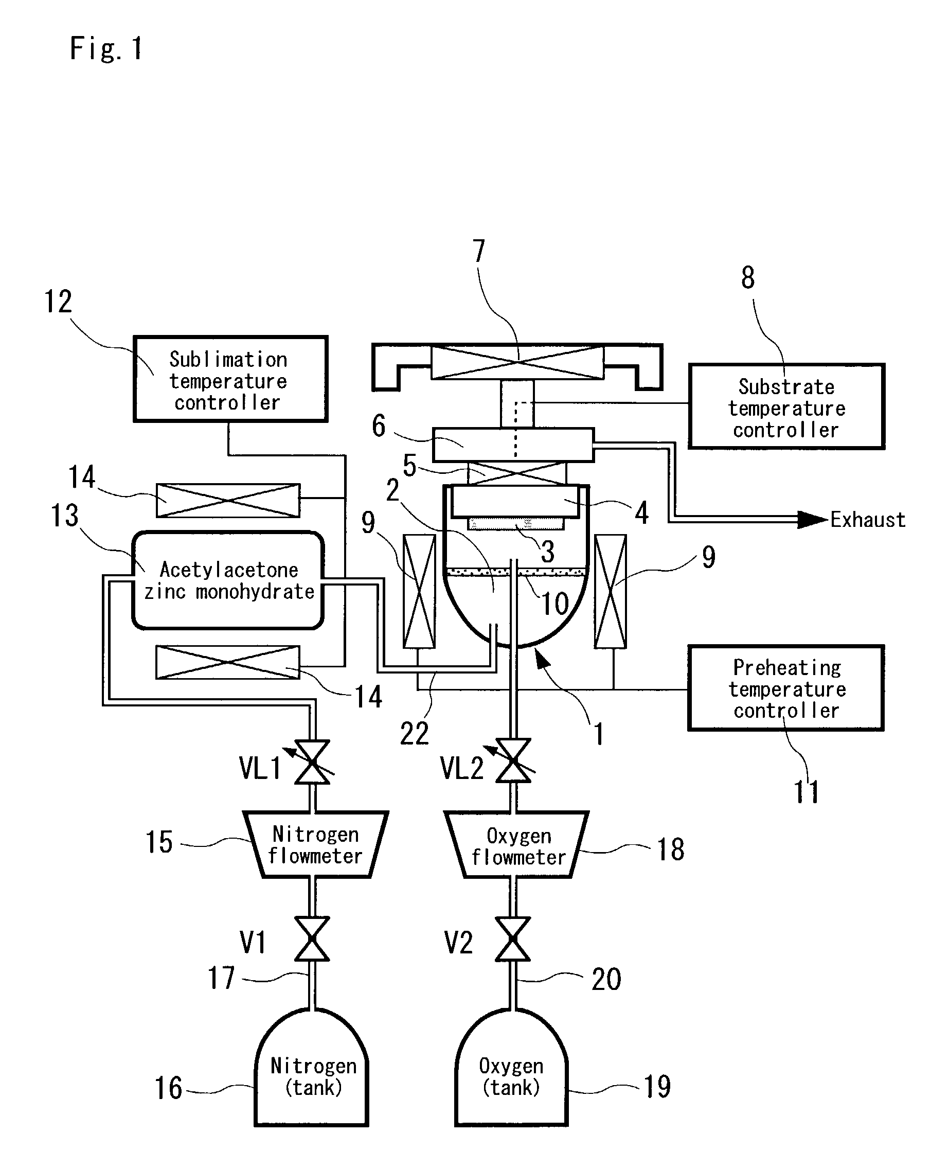
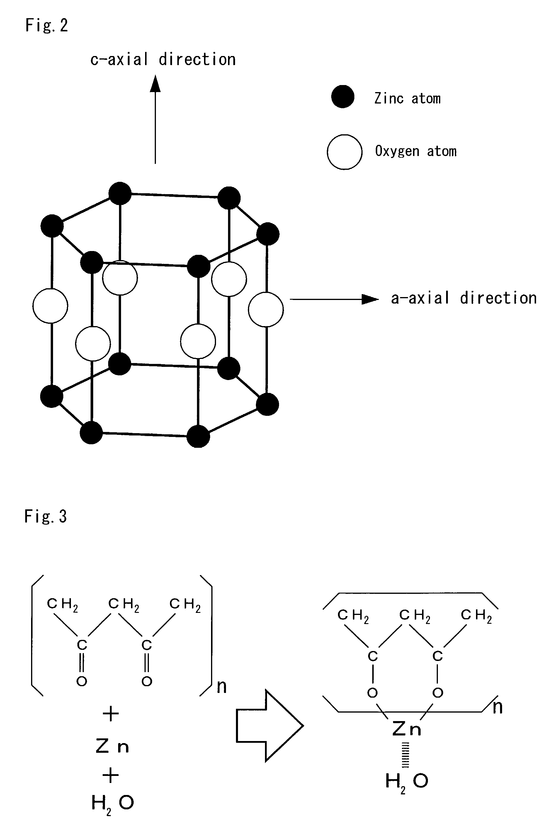
[0057]This example is an application example of a ZnO layer to an external excitation luminescence device. For the substrate 3 for forming the ZnO layer, a single crystal sapphire R-plane was used. Zinc acetylacetonate [Zn(C5H7O2)2] of purity 99.99% was used as a zinc source organic compound, and O2 gas of purity 99.99% was used as an oxygen source. The ZnO layer growth condition was set to a substrate temperature of 475° C., an oxygen flow rate of 400 cc / min, and a nitrogen flow rate as carrier gas of 200 cc / min. The sublimation and preheating were carried out at 124° C. as the set temperature of the sublimation temperature controller 12 and at 160° C. as the set temperature of the preheating temperature controller 11, respectively. The temperatures of the sublimation and preheating may be properly selected on the basis of the kind or reactivity of the zinc-containing organic compound to be used.

[0058]The structural evaluation and surface observation of the ZnO layer thus formed on...


PUM

PropertyMeasurementUnit
TGaaaaaaaaaa
TGaaaaaaaaaa
TGaaaaaaaaaa

Abstract

A zinc oxide semiconductor material comprising at least zinc and oxygen as constituent elements, which can be deterred with respect to the deterioration of doping characteristic, luminous characteristic and the like, compared with a conventional c-axial oriented one by orienting the crystal orientation plane to a-axis of the wurtzite structure.

Description

FIELD OF THE INVENTION[0001]This invention relates to improvements in a zinc oxide semiconductor material comprising at least zinc and oxygen as constituent elements, applied for light emitting in the region of blue and near ultraviolet.BACKGROUND OF THE INVENTION[0002]Zinc oxide semiconductor materials comprising zinc and oxygen as constituent elements have recently attracted considerable attention since they can emit not only blue light but also near ultraviolet rays of 400 nanometers or less because of their wide band gap similarly to semiconductor materials such as gallium nitride and the like. Further, their applications to photodetector, piezoelectric device, transparent conductive electrode, active device and the like have also been expected without being limited to light emitting device.[0003]To form such zinc oxide semiconductor materials, various methods such as MBE method using ultra-high vacuum, sputtering, vacuum evaporation, sol-gel process, MO-CVD method, and the like...

Claims


Application Information

Patent Timeline
Patent Type & Authority Patents(United States)
IPC IPC(8): C30B25/02H01G9/20H01L33/28
CPCC30B25/02H01G9/2027C30B29/16Y02E10/542
Inventor HAGA, KOICHI
Owner TOHOKU TECHNO ARCH CO LTD
Why Eureka
Try Eureka