Method of manufacturing semiconductor device and semiconductor device

a semiconductor and manufacturing method technology, applied in the direction of semiconductor devices, electrical equipment, nanotechnology, etc., can solve the problems of difficult low-voltage operation, and achieve the effects of high selectivity, low power consumption, and high integration

Inactive Publication Date: 2005-08-30
KK TOYOTA CHUO KENKYUSHO
View PDF37 Cites 14 Cited by
  • Summary
  • Abstract
  • Description
  • Claims
  • Application Information

AI Technical Summary

Benefits of technology

[0018]As described above, the present invention makes possible the formation of a very sharp and thin conic body. This conic body is formed with the micro mask used as the top by forming the precipitation area, which is to be the micro mask, in the substrate and performing the anisotropic etching. Therefore, a conic body smaller than the limit of exposure resolution of photolithography or the like can also be formed with ease.
[0057]As described above, the present invention can secure a large capacitor capacity in a small area because the silicon crystal needle is formed on a memory cell and the capacitor on the side face of the needle. Besides, the occupied area on the memory cell can be decreased substantially by forming the switching transistor on the needle. The needle having an appropriate shape and structure is obtained by the anisotropic etching method using the aforesaid micro mask. Thus, the semiconductor memory can be integrated highly, and DRAM of G-bit class can be realized.

Problems solved by technology

This is true because a large radius of curvature at the leading end provides a high electron emission resistance and a large parasitic capacitance with a driving electrode at a gate or the like, making a low voltage operation difficult.

Method used


Image

  • Method of manufacturing semiconductor device and semiconductor device
  • Method of manufacturing semiconductor device and semiconductor device
  • Method of manufacturing semiconductor device and semiconductor device

Examples


embodiment 1

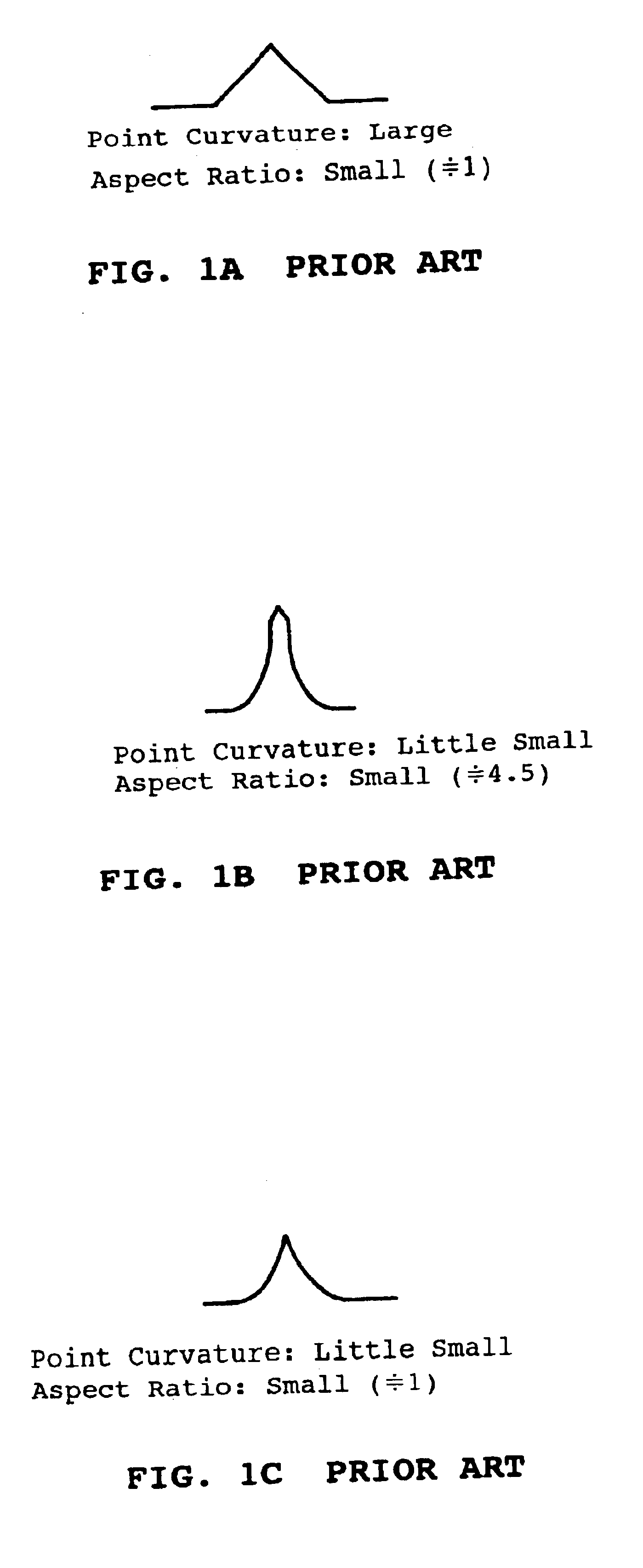
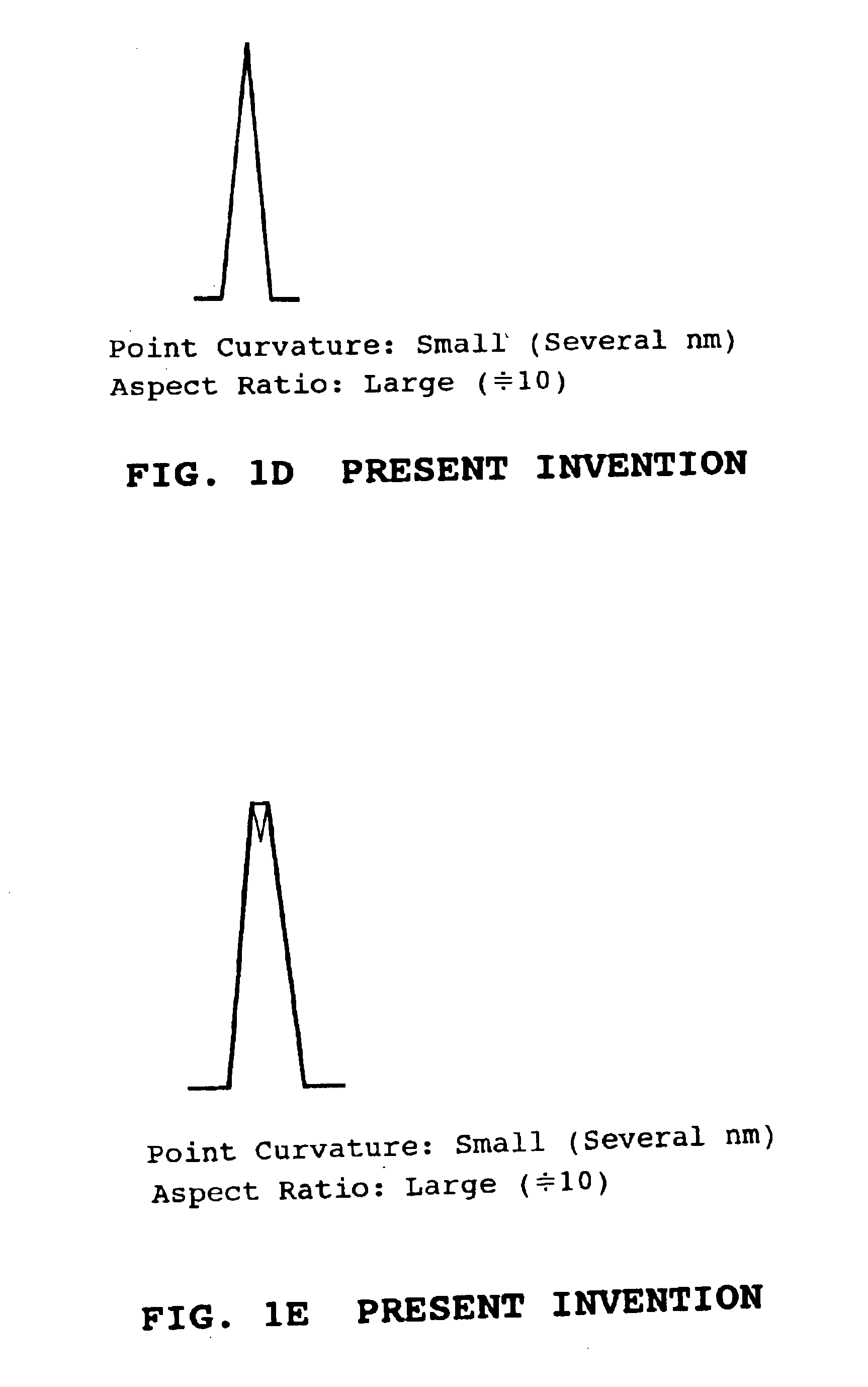
[0102]The conic body of the present invention can be formed by forming an impurity precipitation region in a specific region of a semiconducting material substrate or a predetermined semiconducting material layer and performing high selectivity anisotropic etching with the impurity precipitation region used as a micro mask. Thus, the conic body is formed on the surface exposed by etching with the micro mask used as the top. The conic body in the following embodiment is a cone as an example, and the conic body in the following description will be illustrated with reference to a cone. However, the conic body herein referred to is not limited to a cone, but intended to include every kind of pyramid.

[0103]FIGS. 3A, 3B, 3C and 3D show an example of a method for manufacturing the aforesaid conic body. The following description will be made with reference to a case that a silicon substrate is used as the semiconducting material substrate, and oxygen is introduced as impurities into the sil...

embodiment 2

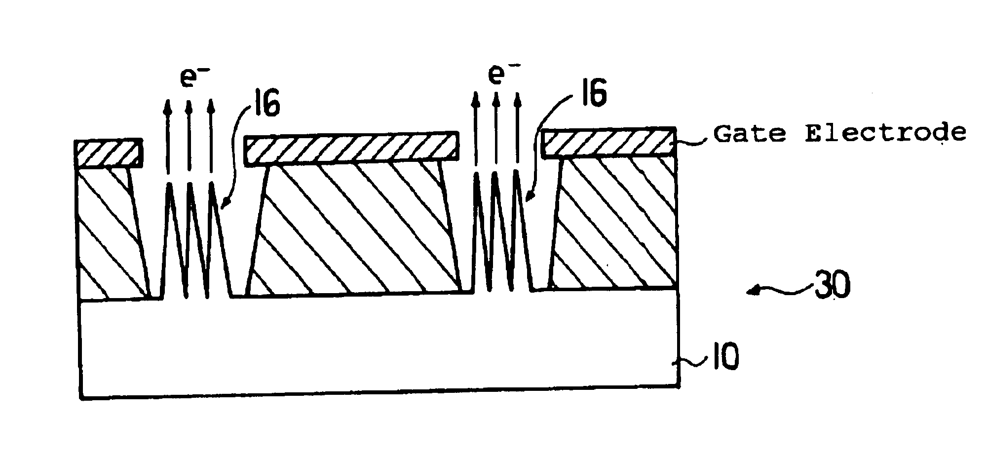
[0127]A process of manufacturing the cone of the present invention obtained by the aforesaid method when it is used for a semiconductor device, e.g., a field emission device or an electron gun will next be described with reference to FIGS. 7A, 7B and 7C. The process shown in FIGS. 7A, 7B and 7C is performed subsequent to the process of FIG. 3D.

[0128]A cone 16 is formed on a silicon substrate 10, a sidewall protective film is removed in the same way as in Embodiment 1 (FIG. 3D), and SiO2 layer 18 is formed as an insulation layer to bury the Si cone 16 as shown in FIG. 7A. In Embodiment 2, for example, to form a polycrystalline silicon (poly-Si) film as a gate electrode on the SiO2 film 18 in the next step, a thickness of the SiO2 layer 18 to be formed is, larger than a height of the Si cone 16, e.g., about 10 nm larger than the thickness of the Si cone 16, so that the leading end of the Si cone 16 is not etched when the poly-Si is patterned.

[0129]After forming the SiO2 layer 18 to a ...

embodiment 3

[0134]FIG. 9 schematically shows a frustum according to Embodiment 3 of the present invention. The conic body in Embodiment 3 is a cone, and the following description in connection with the frustum will be made with reference to a truncated cone. In FIG. 9, (a) shows a structure of the truncated cone seen from its side, and (b) shows a plane structure of the same truncated cone seen from above its leading end. And, the truncated cone has its top removed in the shape of a mortar so to have an annular shape at its leading end. A frustum other than the truncated cone has an annular shape (e.g., a corresponding polygonal annular shape when the frustum is a polygonal prismoid) along its sidewall at the leading end.

[0135]An impurity precipitation region is formed on a particular region in a semiconducting material substrate or a predetermined semiconducting material layer to form a micro mask, and high selectivity anisotropic etching is applied to the micro mask to form the truncated cone...


PUM

PropertyMeasurementUnit
aspect ratioaaaaaaaaaa
diameteraaaaaaaaaa
thicknessaaaaaaaaaa

Abstract

An impurity precipitation region is formed by introducing an impurity, e.g., oxygen, into a silicon substrate or a silicon layer and thermally treating it, and performing high selectivity anisotropic etching with the precipitation region used as a micro mask. Thus, a cone (conic body or truncated conic body having an annular leading end) having a very sharp and slender needle shape with an aspect ratio of about 10 and a diameter of about 10 nm to 30 nm in the vicinity of its leading end is obtained with the micro mask used as the top. By forming an insulation layer and a drive electrode such as a gate electrode around the cone, the cone can be used for a field emission device, a single electron transistor, a memory device, a high frequency switching device, a probe of a scanning type microscope or the like.

Description

[0001]This application is a division of application Ser. No. 09 / 420,524 filed on Oct. 18, 1999, abandoned.BACKGROUND OF THE INVENTION[0002]The present invention relates to a semiconductor device and method of manufacture, particularly to a minute conic (circular, elliptical, poly-hedral) body having a high aspect ratio, and especially to a conic body which can be used in an FED (field emission display or device), a quantum effect device, a memory device, a high frequency device, a probe of scanning type microscope, and the like.DESCRIPTION OF THE RELATED ART[0003]Forming a minute projection on the order of μm on a semiconductor substrate so that the projection may be used for an electron emission source or the like is a known art. Known methods of forming such a minute projection including the method of forming it a cone as shown in FIG. 1A by performing wet etching of a specific crystal plane of a silicon substrate. In “Low voltage silicon minute structure electron source” (Kazuyos...

Claims


Application Information

Patent Timeline
Patent Type & Authority Patents(United States)
IPC IPC(8): H01L21/265H01L21/70H01L21/02H01L29/76H01L29/06H01L21/308H01L29/02H01L21/8242H01L21/335H01L29/788H01L29/66H01L21/3065
CPCB82Y10/00H01L21/26506H01L21/3086H01L27/10864H01L29/0657H01L29/66439H01L29/7613H01L29/7888H01L21/3065H01L21/26566H10B12/0383
Inventor KANECHIKA, MASAKAZUNAKASHIMA, KENJIMITSUSHIMA, YASUICHIKACHI, TETSU
Owner KK TOYOTA CHUO KENKYUSHO
Why Eureka
Try Eureka