

Low-activation energy silicon-containing resist system
a resist system and low activation energy technology, applied in the auxillary/base layer of photosensitive materials, instruments, photosensitive materials, etc., can solve the problems of insufficient resolution capability of many current resists, inability to extend the performance of materials to duv and vuv wavelengths, and inability to manufacture high throughput products. achieve the effect of low activation energy, high optical density, and high resolution transfer of patterned images
- Summary
- Abstract
- Description
- Claims
- Application Information
AI Technical Summary
Benefits of technology
Problems solved by technology
Method used
Image

Examples
example 1
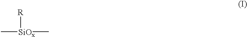
Synthesis of 25% methoxycyclohexene (MOCH) protected poly(2-hydroxy-3,3,3-trifluoropropylsilsesquioxane) (FSQ-25% MOCH)
[0075]25 g of 20 wt. % poly(2-hydroxy-3,3,3-trifluoropropylsilsesquioxane) in PGMEA solution was added in with approximately 35 mg of oxalic acid. After the acid was dissolved, 1.54 g of 1-methoxycyclohexene was added to the solution, and the reaction was carried out at room temperature with stirring overnight. The reaction was then quenched with 5 g of basic active aluminum oxide. The protection level of 25% on fluorocarbinol group was determined by C13 NMR.
example 2
Synthesis of 40% methoxycyclohexene (MOCH) protected poly(2-hydroxy-3,3,3-trifluoropropylsilsesquioxane) (FSQ40% MOCH)
[0076]100 g of 20 wt. % poly(2-hydroxy-3,3,3-trifluoropropylsilsesquioxane) in PGMEA solution was added with approximately 60 mg of oxalic acid. After the acid was dissolved, 12.56 g of 1-methoxycyclohexene was added to the solution, and the reaction was carried out at room temperature with stirring overnight. The reaction was then quenched with 7.2 g of basic active aluminum oxide. Nitrogen was blown through the flask to substantially remove the MOCH. The protection level of 40% on the fluorocarbinol group was determined by C13 NMR.
example 3
Synthesis of FSQ with protecting groups ethyl vinyl ether (EVE), ethoxycyclohexene (EOCH), methoxypropene (MOP), and dihydropyrane (DHP), protected poly(2-hydroxy-3,3,3-trifluoropropylsilsesquioxane), resulting in FSQ protected polymers FSQ-EVE, FSQ-EOCH, FSQ-MOP and FSQ-THP, respectively.
[0077]The synthetic procedures for different acetal and ketal protected FSQ were carried out the same way as in EXAMPLE 1 with the quantity of materials listed in the Table 1 below. All the reactions were quenched with 1.5 g of Al2O3.
[0078]
TABLE 1FSQ(20%Polymersolid)Protecting groupcatalystNMRFSQ-10 g0.58 g ethyl vinyl˜4.5 mg44%EVEethertrifluoracetic acidprotectionFSQ-10 g0.85 g˜10 mg oxalic acid 8%EOCHethoxycyclohexeneprotectionFSQ-12 g0.56 g ˜5 mg oxalic acid15%MOPmethoxypropeneprotectionFSQ-12 g0.70 g ˜5 mg—THPdihydropyranetrifluoroacetic acid
PUM
| Property | Measurement | Unit |
|---|---|---|
| activation energy | aaaaa | aaaaa |
| Ea | aaaaa | aaaaa |
| wavelengths | aaaaa | aaaaa |
Abstract
Description
Claims
Application Information