Method of manufacturing a semiconductor device that includes heating the gate insulating film

a technology of gate insulating film and manufacturing method, which is applied in the direction of semiconductor devices, electrical appliances, transistors, etc., can solve the problems of unfavorable silicon of the catalyst materials enumerated above, and achieve the effect of shortening the duration of tim

Inactive Publication Date: 2005-09-06
SEMICON ENERGY LAB CO LTD
View PDF61 Cites 19 Cited by
  • Summary
  • Abstract
  • Description
  • Claims
  • Application Information

AI Technical Summary

Benefits of technology

[0027]As a result of an extensive study of the present inventors, it has been found that the crystallization of a substantially amorphous silicon film can be accelerated by adding a trace amount of a catalyst material. In this manner, the crystallization can be effected at a lower temperature and in a shorter duration of time. Preferred catalyst materials include pure metals, i.e., nickel (Ni), iron (Fe), cobalt (Co), and platinum (Pt), or a compound such as a silicide of an element enumerated herein. More specifically, the process according to the present invention

Problems solved by technology

The catalyst materials enumerated above,

Method used


Image

  • Method of manufacturing a semiconductor device that includes heating the gate insulating film
  • Method of manufacturing a semiconductor device that includes heating the gate insulating film
  • Method of manufacturing a semiconductor device that includes heating the gate insulating film

Examples


example 1

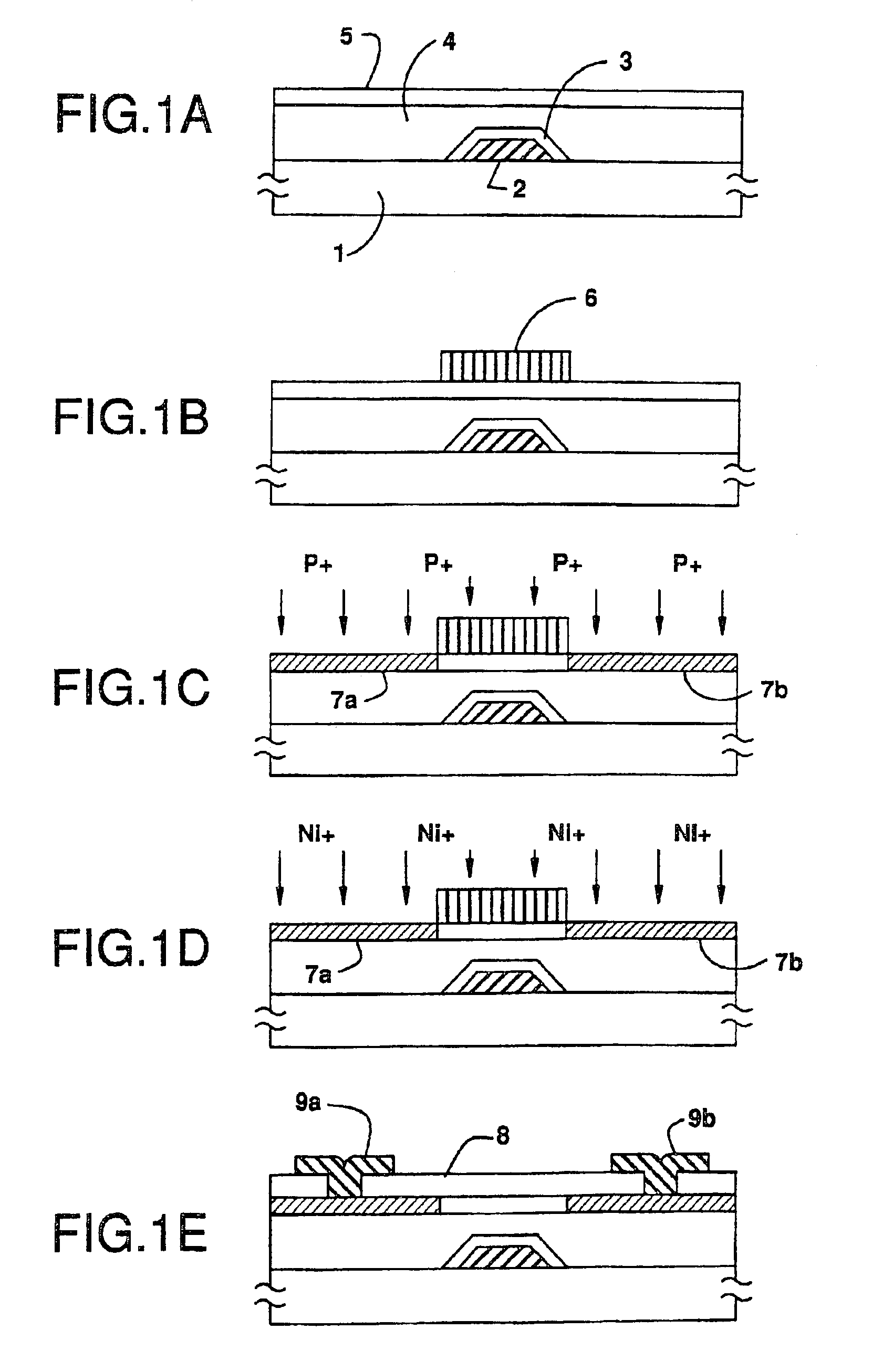
[0074]FIG. 1 shows the cross section view of the step sequential structures obtained by a process according to an embodiment of the present invention. Referring to FIG. 1, a tantalum film was formed at a thickness of from 3,000 to 8,000 Å, for example, at a thickness of 5,000 Å on a Corning #7059 glass substrate 1, and was patterned to form a gate electrode 2. Then, an anodic oxide film 3 was formed at a thickness of from 1,000 to 3,000 Å, for example, at a thickness of 2,000 Å by anodically oxidizing the surface of the tantalum film. Then, a silicon nitride film 4 was deposited by plasma CVD at a thickness of from 1,000 to 5,000 Å, for example, at a thickness of 1,500 Å. This step was followed by the deposition of an intrinsic (I-type) amorphous silicon film thereon by plasma CVD to a thickness of from 200 to 1,500 Å, for example, to a thickness of 500 Å in this case. The resulting amorphous silicon film was patterned to obtain a semiconductor region 5 as shown in FIG. 1(A).

[0075]T...

example 2

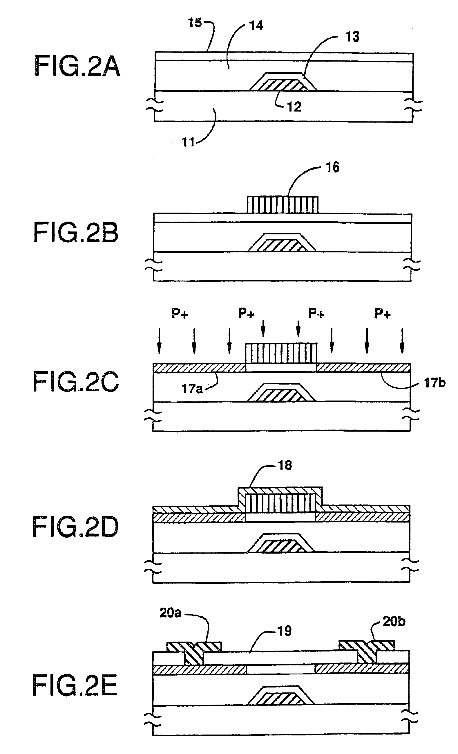
[0081]FIG. 2 shows the cross section view of the step sequential structures obtained by a process according to an embodiment of the present invention. Referring to FIG. 2, a tantalum film was formed at a thickness of from 3,000 to 8,000 Å, for example, at a thickness of 5,000 Å on a Corning #7059 glass substrate 11, and was patterned to form a gate electrode 12. Then, an anodic oxide film 13 was formed at a thickness of from 1,000 to 3,000 Å, for example, at a thickness of 2,000 Å by anodically oxidizing the surface of the tantalum film. Then, a silicon nitride film 14 was deposited by plasma CVD at a thickness of from 1,000 to 5,000 Å, for example, at a thickness of 1,500 Å. This step was followed by the deposition of an intrinsic (I-type) amorphous silicon film thereon by plasma CVD to a thickness of from 200 to 1,500 Å, for example, to a thickness of 500 Å in this case. The resulting amorphous silicon film was patterned to obtain a semiconductor region 15 as shown in FIG. 2(A).

[0...

example 3

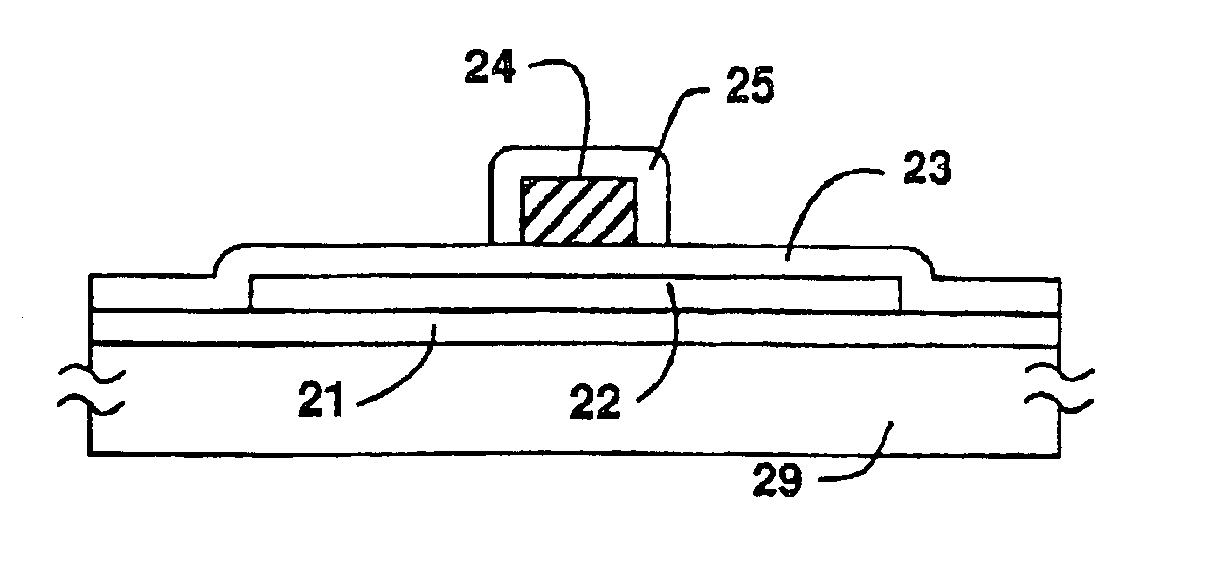
[0088]FIG. 3 shows the cross section view of the step sequential structures obtained by a process according to another embodiment of the present invention. Referring to FIG. 3, a 2,000 Å thick silicon oxide film ill was formed by sputtering as a base film on a Corning #7059 glass substrate 110. Then, an intrinsic (I-type) amorphous silicon film was deposited thereon by plasma CVD to a thickness of from 500 to 1,500 Å, for example, to a thickness of 1,500 Å. The amorphous silicon film was then crystallized by annealing at 600° C. in nitrogen atmosphere for a duration of 48 hours. After annealing, the silicon film was patterned to form an island-like silicon region 112, and a 1,000 Å thick silicon oxide film 113 was deposited thereon by sputtering as a gate insulating film. The sputtering process was performed in an atmosphere containing oxygen and argon at an argon to oxygen ratio of not higher than 0.5, for example, at a ratio of 0.1 or lower, using silicon oxide as the target. The,...


PUM


Abstract

A process for fabricating a thin film transistor, which comprises crystallizing an amorphous silicon film, forming thereon a gate insulating film and a gate electrode, implanting impurities in a self-aligned manner, adhering a coating containing a catalyst element which accelerates the crystallization of the silicon film, and annealing the resulting structure at a temperature lower than the deformation temperature of the substrate to activate the doped impurities. Otherwise, the catalyst element can be incorporated into the structure by introducing it into the impurity region by means of ion implantation and the like. Also a process for fabricating a thin film transistor, which comprises forming a gate electrode, a gate insulating film, and an amorphous silicon film on a substrate, implanting impurities into the amorphous silicon film to form source and drain regions as the impurity regions, introducing a catalyst element into the impurity region by adhering a coating containing the catalyst element of by means of ion doping and the like, and annealing the resulting structure at a temperature lower than the deformation temperature of the substrate to activate the doped impurities.

Description

BACKGROUND OF THE INVENTION[0001]1. Field of the Invention[0002]The present invention relates to a thin film transistor (TFT) and a process for fabricating the same. The thin film transistor fabricated according to the present invention can be formed on either an insulator substrate such as a glass substrate or a substrate made of, for example, a crystalline silicon. In particular, the present invention relates to a thin film transistor fabricated through steps of crystallization and activation by thermal annealing.[0003]2. Prior Art[0004]Recently, active study is made on semiconductor devices of insulated-gate type comprising an insulator substrate having thereon a thin film active layer (which is sometimes referred to as “active region”). In particular, much effort is paid on the study of insulated-gate transistors of thin film type, i.e., the so-called thin film transistors (TFTs). The TFTs are formed on a transparent insulator substrate, so that they can be employed mainly for c...

Claims


Application Information

Patent Timeline
IPC IPC(8): H01L21/265H01L29/66H01L21/02H01L29/786H01L21/336H01L21/20H01L29/49H01L29/40H01L21/324H01L29/78
CPCH01L21/2022H01L21/26506H01L29/4908H01L29/66757H01L29/66765H01L29/78618H01L29/78675H01L29/78678H01L21/02488H01L21/02491H01L21/02422H01L21/02532H01L21/02505H01L21/02672
Inventor ZHANG, HONGYONGTAKAYAMA, TORUTAKEMURA, YASUHIKO
Owner SEMICON ENERGY LAB CO LTD
Why Eureka
Try Eureka