Packaging system for power supplies

a power supply and power supply technology, applied in the direction of semiconductor devices, semiconductor/solid-state device details, electrical apparatus, etc., can solve the problems of power supply packaging technology that has not kept pace with the ics, power supply and power supply power supply consumption is increasing. , to achieve the effect of low resistance, low current control signal, and high current connection

Inactive Publication Date: 2005-09-13
PWER BRIDGE
View PDF6 Cites 29 Cited by
  • Summary
  • Abstract
  • Description
  • Claims
  • Application Information

AI Technical Summary

Benefits of technology

[0007]The present disclosure is directed to a package (housing) for a power supply or other circuit involving high electric current, which couples low resistance, high current metallic posts (leads) directly to the current-handling input and output electrodes of the die of the semiconductor devices, which are, e.g. switching transistors (such as FETs). The posts are the pins (external leads) of, e.g. a single-in-line package (SIP), and are held in place by attaching them mechanically to a substrate such as a rigid printed circuit board. The circuit board conventionally provides a substrate for the FETs and supporting circuitry, for example a controller chip which operates the transistors and associated fil

Problems solved by technology

Future processors may consume current at levels an order of magnitude higher than today's processors, and will dissipate much more power because the operating voltage will not decrease proportionately.
The packaging requirements for such power FETs and power supplies are demanding, as they must switch high currents in a small physical size.
However, circuit assembly and packaging technology for power supplies have not kept pace with those of ICs.
The state-of-the-art packaged power supplies are in the forms of single-in-line package (SIP), dual-in-line package (DIP), small outline package (SO or SOP) and quad flat pack (QFP), which have undesirably large size, high resistance and parasitic capacitance, poor thermal management and high cost.
Such wire bonds are prone to resistance, noise, parasitic capacitance and inductance, fatigue

Method used


Image

  • Packaging system for power supplies
  • Packaging system for power supplies
  • Packaging system for power supplies

Examples


Embodiment Construction

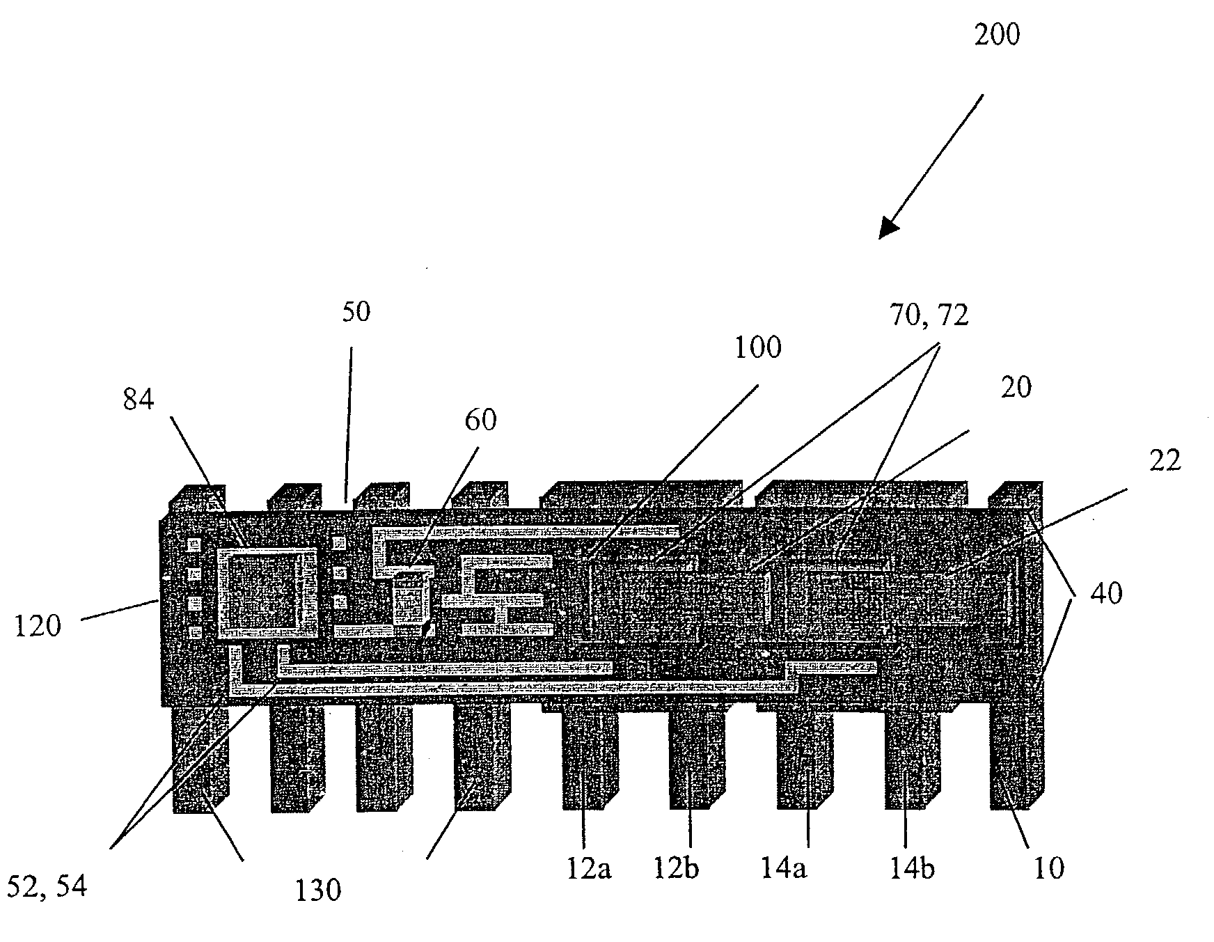
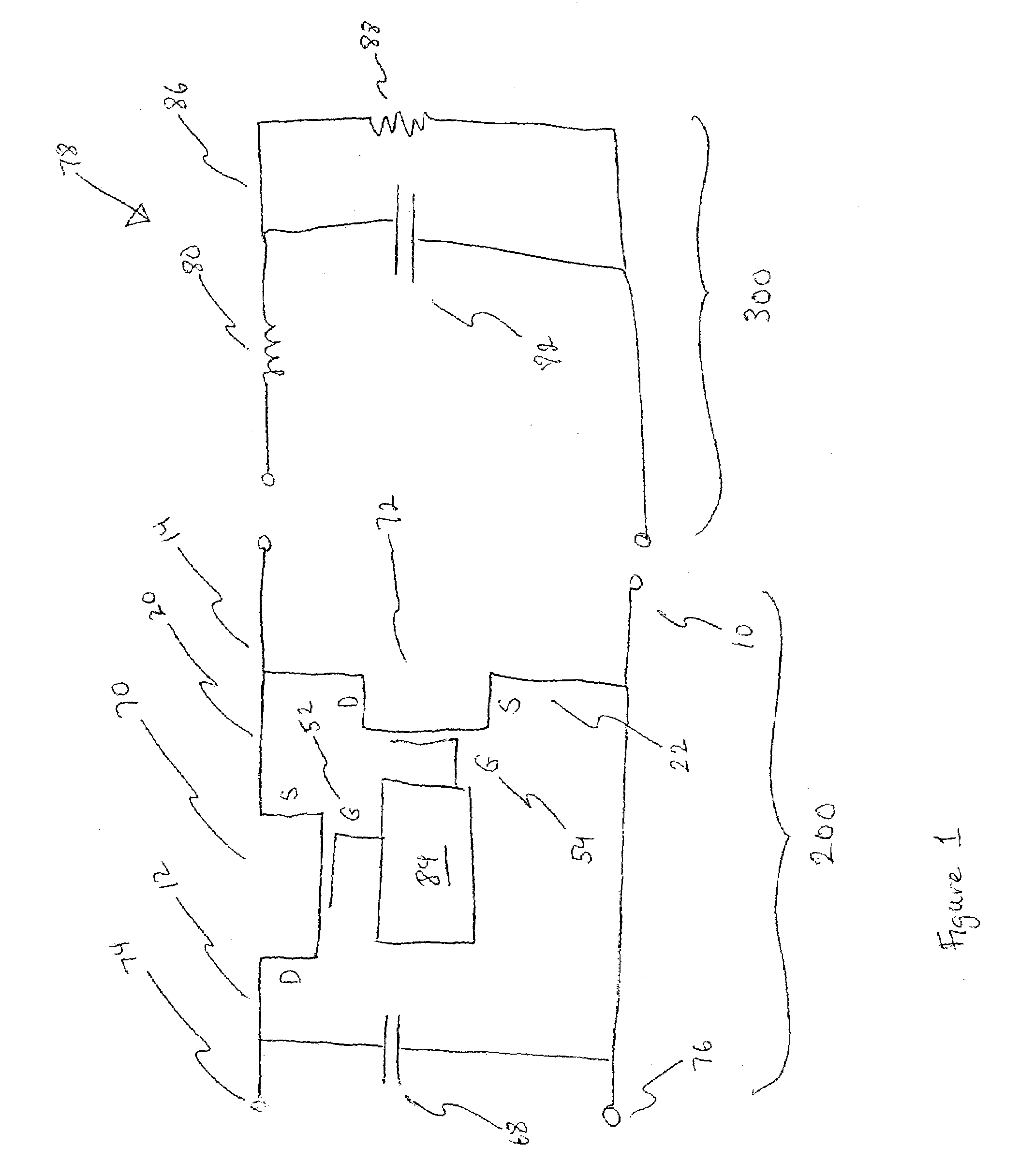
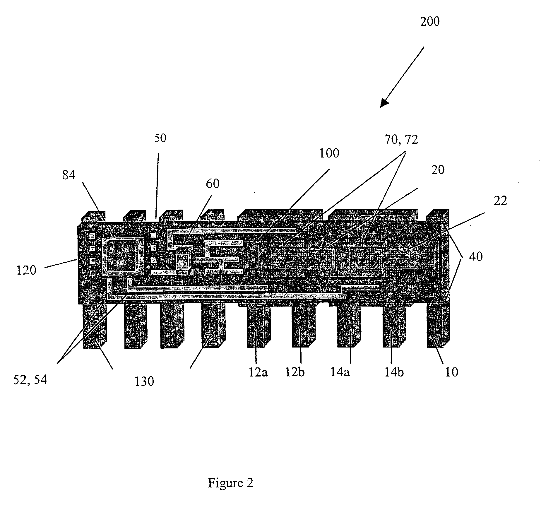
[0017]This disclosure is directed to a package in which contact is made to the electrodes of a “bare die” (unpackaged) semiconductor device such as a power transistor (switch), by connecting low resistance, high current conductive posts directly to the current input and output electrodes of the power transistor. The posts are held in place by attaching them mechanically to a printed circuit board or other substrate on which the transistor is also mounted, and are the leads to electrically connect the transistor externally to the package. The circuit board also provides a substrate for supporting circuitry, for example the controller chip which operates the transistor switches. However the traces of the printed circuit board need carry no high current, as high current paths are defined by the posts. Additional high current connections internal to the package, are via relatively thick metallic “straps” coupled to the transistors and posts using, e.g. conductive epoxy or solder paste. ...


PUM


Abstract

A packaging system for a high current, low voltage power supply. The power supply uses two bare die field effect transistors whose input and output electrodes are solder attached to low resistance, high current posts in the package. An associated controller chip is mounted to a rigid circuit board, and the circuit board is mechanically attached to the posts. The circuit board thereby gives physical rigidity to the package, but carries no high currents. The use of low resistance, high current posts reduces the heat generated, improving the long term reliability.

Description

FIELD OF THE INVENTION[0001]The present invention relates to the packaging of integrated circuits and semiconductor devices. More particularly, this invention relates to the packaging of high power field effect transistors or other semiconductor devices for power supplies.BACKGROUND OF THE INVENTION[0002]With the advent of microprocessors and other electronics that consume more electrical power, comes the need for higher output current power supplies. While microprocessor voltage requirements are decreasing, substantial increases in electric current requirements are offsetting this trend. Future processors may consume current at levels an order of magnitude higher than today's processors, and will dissipate much more power because the operating voltage will not decrease proportionately. GHz class central processing units (CPUs) are routinely specified to draw 30A or more of direct current. Therefore a need has arisen for high current, low voltage power sources which have a small phy...

Claims


Application Information

Patent Timeline
IPC IPC(8): H01L21/02H01L23/34H01L23/48H01L23/40H01L23/52H01L21/31H01LH01L21/60H01L21/607H01L23/495H01L23/50
CPCH01L23/49524H01L23/49562H01L23/50H01L24/40H01L24/49H01L24/73H01L24/91H01L24/45H01L24/83H01L2224/45124H01L2224/48091H01L2224/48247H01L2224/48465H01L2224/4903H01L2224/49051H01L2224/73221H01L2224/73265H01L2224/83801H01L2224/83851H01L2224/84205H01L2924/01013H01L2924/01014H01L2924/01015H01L2924/01028H01L2924/01029H01L2924/01049H01L2924/01078H01L2924/01079H01L2924/01082H01L2924/10253H01L2924/13091H01L2924/14H01L2924/19041H01L2924/19042H01L2924/19043H01L2924/30105H01L2924/30107H01L24/48H01L2224/32245H01L2924/01005H01L2924/01033H01L2924/014H01L2224/37147H01L2224/2929H01L2224/293H01L2924/00011H01L2924/1306H01L2924/1305H01L2924/00014H01L2924/00012H01L2924/00H01L2924/3512H01L2224/29075H01L2924/181H01L2224/40095H01L2224/40245H01L24/37H01L2224/84801H01L2224/8385H01L2224/8485H01L24/84H01L2224/83205
Inventor MAXWELL, JOHN A.
Owner PWER BRIDGE
Why Eureka
Try Eureka