Film forming method and film forming device

a film forming and film technology, applied in the direction of chemistry apparatus and processes, coatings, plasma techniques, etc., can solve the problems of film adhesion, mechanical and chemical resistance and thermal conductivity problems, and the capacitance between wires has posed problems, and achieve excellent mechanical and chemical resistance, excellent moisture absorption resistance, and high thermal conductivity.

Inactive Publication Date: 2005-10-25
M WATANABE CO LTD
View PDF7 Cites 234 Cited by
  • Summary
  • Abstract
  • Description
  • Claims
  • Application Information

AI Technical Summary

Benefits of technology

[0007]Because of this feature, a boron nitride film excellent in mechanical and chemical resistance, high in thermal conductivity, and having a low relative dielectric constant κ can be formed speedily.
[0009]Because of this feature, a boron carbonitride film excellent in moisture-absorption resistance, excellent in mechanical and chemical resistance, high in thermal conductivity, and having a low relative dielectric constant κ can be formed speedily.
[0013]Because of this feature, a plasma is generated within a film formation chamber, mainly a nitrogen gas is excited within the film formation chamber, and then the excited nitrogen gas is mixed with a diborane gas diluted with a hydrogen gas, to react them, thereby forming a boron nitride film on a substrate. As a result, a boron nitride film excellent in mechanical and chemical resistance, high in thermal conductivity, and having a low relative dielectric constant κ can be formed speedily.
[0015]Because of this feature, a plasma is generated within a film formation chamber, mainly a nitrogen gas is excited within the film formation chamber, and then the excited nitrogen gas is reacted with a diborane gas diluted with a hydrogen gas, and an organic gas, thereby forming a boron carbonitride film on a substrate. As a result, a boron carbonitride film excellent in moisture absorption resistance, excellent in mechanical and chemical resistance, high in thermal conductivity, and having a low relative dielectric constant κ can be formed speedily.

Problems solved by technology

However, because of high integration of transistors and speeding of a switching action, losses due to capacitance between wirings have posed problems.
Under these circumstances, films of organic materials (for example, organosilicon films or films of amorphous carbon incorporating fluorine) can be provided with a very low relative dielectric constant (relative dielectric constant κ=2.5 or less), but these films have been problematical in mechanical and chemical resistance and thermal conductivity.
Adhesion of the films has also presented a problem, and their moisture absorption resistance has been a problem in terms of density.
However, techniques for forming a BN film or a BNC film by the plasma CVD (chemical vapor deposition) method have not been established, and the advent of a film forming method and a film forming apparatus capable of forming a BN film and a BNC film as products is in eager demand.

Method used


Image

  • Film forming method and film forming device
  • Film forming method and film forming device
  • Film forming method and film forming device

Examples


Embodiment Construction

[0021]To describe the present invention in more detail, the invention will be illustrated in accordance with the accompanying drawings.

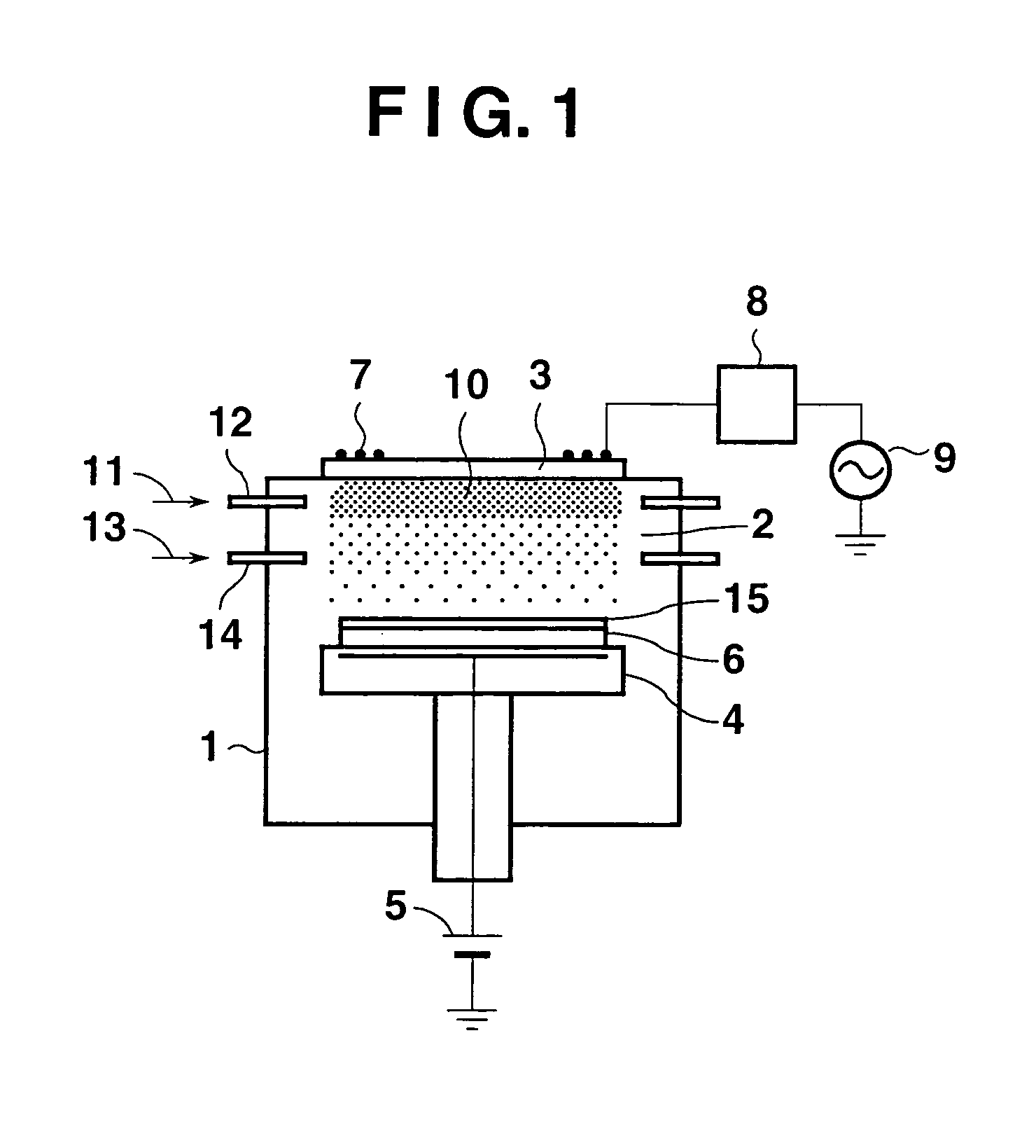
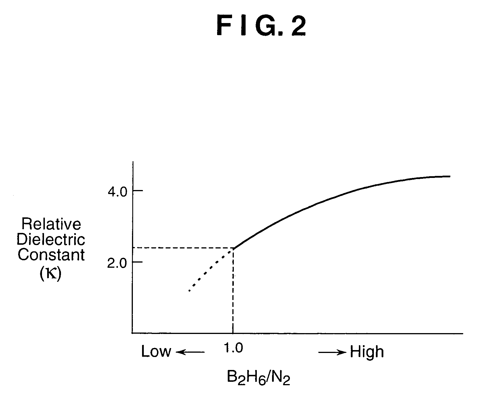
[0022]The first embodiment is explained based on FIGS. 1 and 2. FIG. 1 schematically shows a side view of a plasma CVD apparatus as a film forming apparatus for performing the film forming method according to the first embodiment of the present invention. FIG. 2 shows a graph representing the relationship between the ratio of diborane to nitrogen and the relative dielectric constant.

[0023]As shown in FIG. 1, a film formation chamber 2 is formed within a cylindrical container 1, and a circular ceiling board 3 is provided in an upper part of the container 1. An electrostatic chuck 4, as a substrate holding portion, is provided in the film formation chamber 2 at the center of the container 1. A direct current power source 5 for the electrostatic chuck is connected to the electrostatic chuck 4 so that a substrate 6 of a semiconductor is electrostatically...


PUM

PropertyMeasurementUnit
temperatureaaaaaaaaaa
frequencyaaaaaaaaaa
relative dielectric constantaaaaaaaaaa

Abstract

A plasma 10 is generated within a film formation chamber 2, and mainly a nitrogen gas 11 is excited within the film formation chamber 2. Then, the excited nitrogen gas 11 is reacted with a diborane gas 13 diluted with a hydrogen gas, thereby forming a boron nitride film 15 on a substrate 4. Thus, the boron nitride film 15 excellent in mechanical and chemical resistance, high in thermal conductivity, and having a low relative dielectric constant κ can be formed speedily.

Description

[0001]This application is the national phase under 35 U.S.C. § 371 of PCT International Application No. PCT / JP02 / 03071 which has an International filing date of Mar. 28, 2002, which designated the United States of America.TECHNICAL FIELD[0002]This invention relates to a film forming method and a film forming apparatus for forming a boron nitride film and a boron carbonitride film.BACKGROUND ART[0003]In an integrated circuit, a silicon dioxide film (SiO2 film) by the plasma CVD (chemical vapor deposition) method has so far been used as an interlayer dielectric film. However, because of high integration of transistors and speeding of a switching action, losses due to capacitance between wirings have posed problems. To eliminate these losses, it is necessary to decrease the relative dielectric constant of the interlayer dielectric film, so that an interlayer dielectric film with a lower relative dielectric constant has been demanded. Under these circumstances, films of organic material...

Claims


Application Information

Patent Timeline
Patent Type & Authority Patents(United States)
IPC IPC(8): C04B35/583C23C16/30C23C16/34C23C16/36H01L21/02H01L21/318C01B21/082C01B21/064C23C16/38H01L21/31
CPCC04B35/583C23C16/30C23C16/342C23C16/36H01L21/318H01L21/02274H01L21/02112H01L21/205
Inventor SAKAMOTO, HITOSHIUEDA, NORIAKISUGINO, TAKASHI
Owner M WATANABE CO LTD
Why Eureka
Try Eureka