
DRAM cells with repressed floating gate memory, low tunnel barrier interpoly insulators

a floating gate memory, dram cell technology, applied in the field of integrated circuits, can solve the problems of loss of all knowledge of the state limited memory longevity, and constant refreshing of the dram devi

Inactive Publication Date: 2005-10-25
MICRON TECH INC
View PDF81 Cites 80 Cited by
  • Summary
  • Abstract
  • Description
  • Claims
  • Application Information

AI Technical Summary

Benefits of technology

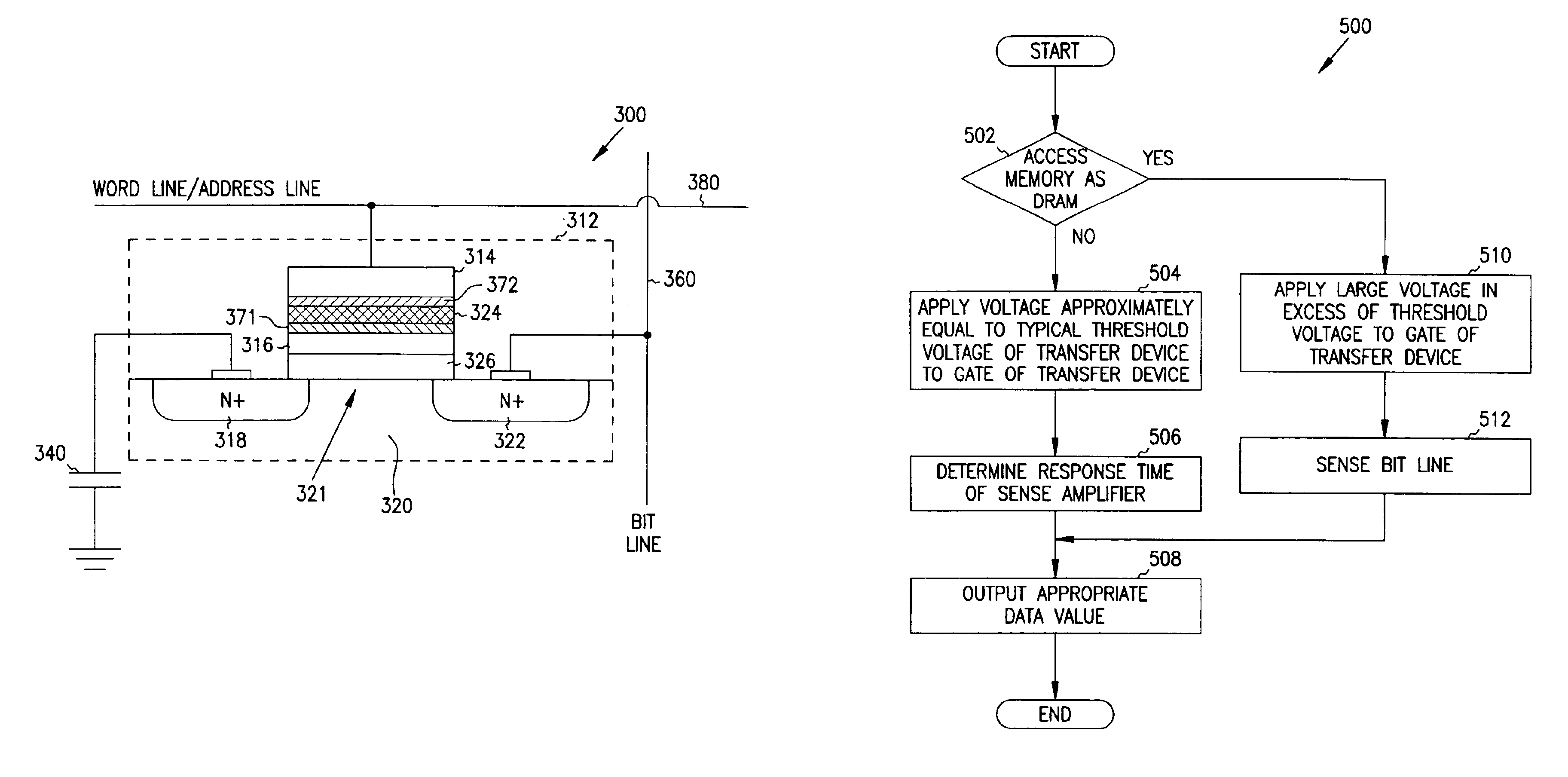
[0042]The above mentioned problems with conventional memories and other problems are addressed by the present invention and will be understood by reading and studying the following specification. Systems and methods are provided for high density memories having both a volatile and non-volatile component. The non-volatile component includes a floating gate separated from a control gate by a metal oxide and / or low tunnel barrier interpoly insulator.

Problems solved by technology

They are, however, limited in the longevity of their memory.
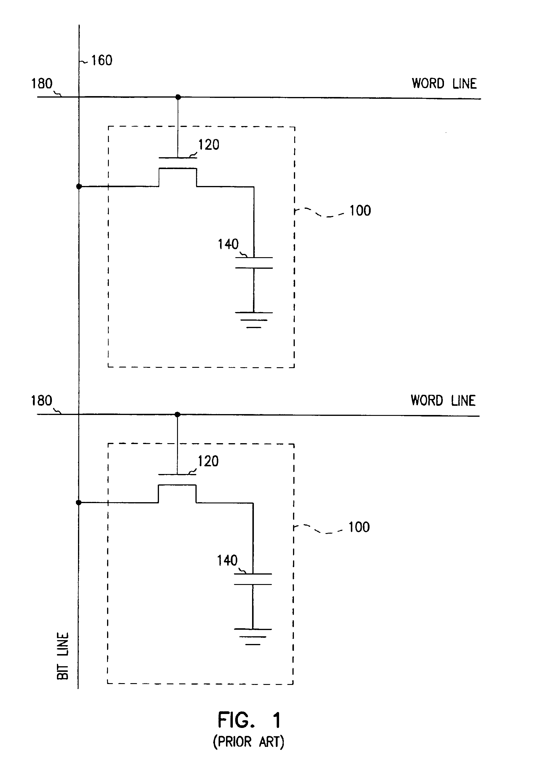
DRAM devices require constant refreshing and lose all knowledge of their state (i.e., contents) once power to the device is removed.
This, however, consumes valuable chip real estate.
Again, memory separate from the main memory is required, which adds cost and adds to the size and complexity of the system.
Instead, separate cells are used, which adds cost, size and complexity to the memory.
However, the rough top surface of the polysilicon floating gate resulted in, poor quality interpoly oxides, sharp points, localized high electric fields, premature breakdown and reliability problems.
However, in order to enable a reasonable write speed the ETOX cell uses channel hot electron injection, the erase operation which can be slower is achieved by Fowler-Nordhiem tunneling from the floating gate to the source.
The large barriers to electron tunneling or hot electron injection presented by the silicon oxide-silicon interface, 3.2 eV, result in slow write and erase speeds even at very high electric fields.
The combination of very high electric fields and damage by hot electron collisions in the oxide result in a number of operational problems like soft erase error, reliability problems of premature oxide breakdown and a limited number of cycles of write and erase.
The non-volatile memory component should avoid the large barriers to electron tunneling or hot electron injection presented by the silicon oxide-silicon interface, 3.2 eV, which result in slow write and erase speeds even at very high electric fields.
There is also a need, within the non-volatile component, to avoid the combination of very high electric fields and damage by hot electron collisions in the which oxide result in a number of operational problems like soft erase error, reliability problems of premature oxide breakdown and a limited number of cycles of write and erase.
Further, when using an interpoly dielectric insulator erase approach for the non-volatile component, the above mentioned problems of having a rough top surface on the polysilicon floating gate which results in, poor quality interpoly oxides, sharp points, localized high electric fields, premature breakdown and reliability problems must be avoided.

Method used


Image

  • DRAM cells with repressed floating gate memory, low tunnel barrier interpoly insulators
  • DRAM cells with repressed floating gate memory, low tunnel barrier interpoly insulators
  • DRAM cells with repressed floating gate memory, low tunnel barrier interpoly insulators

Examples


example i

Formation of PbO Tunnel Barriers

[0105]This oxide barrier has been studied in detail using Pb / PbO / Pb structures. The oxide itself can be grown very controllably on deposited lead films using either thermal oxidation or rf sputter etching in an oxygen plasma. It will be seen that there are a number of possible variations on this structure. Starting with a clean poly-Si substrate, one processing sequence using thermal oxidation involves:

[0106](i) Depositing a clean lead film on the poly-Si floating gate at ˜25 to 75C in a clean vacuum system having a base pressure of ˜10−8 Torr or lower. The Pb film will be very thin with a thickness within 1 or 2A of its target value.

[0107](ii) Lead and other metal films can be deposited by various means including physical sputtering and / or from a Knudsen evaporation cell. The sputtering process also offers the ability to produce smoother films by increasing the re-sputtering-to-deposition ratio since re-sputtering preferentially reduces geometric hig...

example ii

Formation of Al2O3 Tunnel Barriers

[0111]A number of studies have dealt with electron tunneling in Al / Al2O3 / Al structures where the oxide was grown by “low temperature oxidation” in either molecular or plasma oxygen. Before sketching out a processing sequence for these tunnel barriers, note:

[0112](i) Capacitance and tunnel measurements indicate that the Al2O3 thickness increases with the log (oxidation time), similar to that found for PbO / Pb as well as a great many other oxide / metal systems.

[0113](ii) Tunnel currents are asymmetrical in this system with somewhat larger currents flowing when electrons are injected from Al / Al2O3 interface developed during oxide growth. This asymmetry is due to a minor change in composition of the growing oxide: there is a small concentration of excess metal in the Al2O3, the concentration of which diminishes as the oxide is grown thicker. The excess Al−3 ions produce a space charge that lowers the tunnel barrier at the inner interface. The oxide compos...

example iii

Formation of Single- and Multi-layer Transition Metal Oxide Tunnel Barriers

[0119]Single layers of Ta2O5, TiO2, ZrO2, Nb2O5 and similar transition metal oxides can be formed by “low temperature oxidation” of numerous Transition Metal (e.g., TM oxides) films in molecular and plasma oxygen and also by rf sputtering in an oxygen plasma. The thermal oxidation kinetics of these metals have been studied for decades with numerous descriptions and references. In essence, such metals oxidize via logarithmic kinetics to reach thicknesses of a few to several tens of angstroms in the range of 100 to 300C. Excellent oxide barriers for Josephson tunnel devices can be formed by rf sputter etching these metals in an oxygen plasma. Such “low temperature oxidation” approaches differ considerably from MOCVD processes used to produce these TM oxides. MOCVD films require high temperature oxidation treatments to remove carbon impurities, improve oxide stoichiometry and produce recrystallization. Such high...


PUM


Abstract

Structures and methods for memory cells having a volatile and a non-volatile component in a single memory cell are provided. The memory cell includes a first source / drain region and a second source / drain region separated by a channel region in a substrate. A floating gate opposes the channel region and separated therefrom by a gate oxide. A control gate opposes the floating gate. The control gate is separated from the floating gate by a low tunnel barrier intergate insulator. The memory cell is adapted to operate in a first and a second mode of operation. The first mode of operation is a dynamic mode of operation and the second mode of operation is a repressed memory mode of operation.

Description

RELATED APPLICATIONS[0001]This application is a continuation of U.S. application Ser. No. 09 / 945,395 filed on 30 Aug. 2001, now issued as U.S. Patent No. 6,754,108, which is incorporated herein by reference.CROSS REFERENCE TO RELATED APPLICATIONS[0002]This application is related to the following co-pending, commonly assigned U.S. patent applications: “Programmable Array Logic or Memory Devices with Asymmetrical Tunnel Barriers,” Ser. No. 09 / 943,134, “Integrated Circuit Memory Device and Method,” Ser. No. 09 / 945,498, “In Service Programmable Logic Arrays with Low Tunnel Barrier Interpoly Insulators,” serial number 09 / 945,512, “Flash Memory with Low Tunnel Barrier Interpoly Insulators,” Ser. No. 09 / 945,507, “Programmable Memory Address and Decode Circuits with Low Tunnel Barrier Interpoly Insulators,” Ser. No. 09 / 945,500, and “SRAM Cells with Repressed Floating Gate Memory, Low Tunnel Barrier Interpoly Insulators,” Ser. No. 09 / 945,554, which were filed on Aug. 30, 2001 and each of whi...

Claims


Application Information

Patent Timeline
Patent Type & Authority Patents(United States)
IPC IPC(8): G11C11/404G11C11/403H01L29/40H01L29/423H01L29/51
CPCG11C11/404H01L27/10873H01L29/42324H01L29/511H01L29/7881H10B12/05
Inventor FORBES, LEONARD
Owner MICRON TECH INC
Learn More