Integrated aspheric optical coupler for RF planarized automatic photonics packaging

a technology of automatic photonics and aspheric optical couplers, applied in the field of photonics packages, can solve the problems of reducing device performance at high frequency operation, data can easily be lost, and complicating the assembly process, so as to achieve accurate and reliable alignment of optical fibers, reduce assembly costs, and simple optical coupling

Inactive Publication Date: 2005-11-15
NORTHROP GRUMMAN SYST CORP
View PDF7 Cites 13 Cited by
  • Summary
  • Abstract
  • Description
  • Claims
  • Application Information

AI Technical Summary

Benefits of technology

[0010]A final step for fabricating the alignment device includes metalizing the fiber groove and the bottom of the substrate block, as with solder. Thereafter, an optical fiber having an angled terminal end is secured in the groove with the optical axis of the angled surface of the fiber aligned with the optical axis of the lens, and a photonic die is positioned in the recess so that a photodetector region or a surface light emitting active area on the die is aligned with the optical axis of the lens, and thus with the optical signal axis of the fiber. The monolithic alignment structure assures accurate and reliable alignment of the optical fiber, the lens, and the photodetector or surface light emitting device, and lends itself to automatic assembly procedures.
[0011]Overall, the ability to form a monolithic, compact and simple optical coupling system for micro-optical devices has several advantages. For example, constructing all the components of an alignment device from identical material in a single process lowers assembly costs, reduces alignment problems during assembly and overcomes problems caused in earlier devices by unequal thermal expansion between components. Moreover, complex coupling and alignment schemes can be eliminated, reducing the number of components and the complexity of the process of manufacturing the device. A monolithic structure also permits a closer proximity of the fiber, lens, and photodetector light emitters, which allows for more accurate alignment, a decrease in the time required for alignment, and more efficient packaging of optical electronics systems. The assembly of the package can be automated, resulting in higher volume manufacturing and higher reproducibility.
[0012]In summary, a monolithic micro-optical device incorporating a photonics package in accordance with the present invention efficiently addresses various problems associated with optical communication applications and improves upon the prior art by providing a commercially advantageous product. The device eliminates the need for manual assembly and improves reliability and accuracy by simplifying prior devices.

Problems solved by technology

However, data can easily be lost due to improper alignment between the fiber and the photodetector or through light divergence, although both the alignment and divergence problems can be minimized where the fiber and the photodetector are in close proximity or where a lens can be used to focus the optical signal.
In the first construction, wherein light is projected from fiber directly onto the photodetector, the photodetector and the fiber must be optically aligned in three mutually perpendicular planes ((x-y), (x-z), and (y-z)), which complicates the assembly process.
Moreover, such an arrangement can be problematic for high frequency data transfer because it requires a longer wire bonding or transmission line, and this reduces device performance at high frequency operation.
This design configuration also results in the optical input being perpendicular to the RF signal output, and this requires much more space in a module.
These performance and size issues make this approach commercially less desirable, and this is the disfavored, if not unacceptable, approach for many applications where it is advantageous to have the fiber input and RF output substantially coplanar.
However, there are several problems with this method.
Using a discrete mirror (an additional element needing alignment) introduces an indirect connection between the fiber and photodetector, causing difficulty during alignment, raising costs due to the need for a more precise construction, and reducing reliability.
Further, the three components; namely, the fiber, lens, and photodetector, have to be precisely located with respect to each other to ensure reliable coupling, and this is difficult to accomplish.
In each of the configurations discussed above, the photonic package consists of several independently fabricated micro-optical components, including an optical fiber, a photodetector, a mirror, a lens and and a substrate or microbench on which the components are assembled, as well as bonding materials to connect the components, and frequently all were assembled manually, which is not efficient.
Although automated assembly could be used, it fails to achieve the needed alignment precision.

Method used


Image

  • Integrated aspheric optical coupler for RF planarized automatic photonics packaging
  • Integrated aspheric optical coupler for RF planarized automatic photonics packaging
  • Integrated aspheric optical coupler for RF planarized automatic photonics packaging

Examples


Embodiment Construction

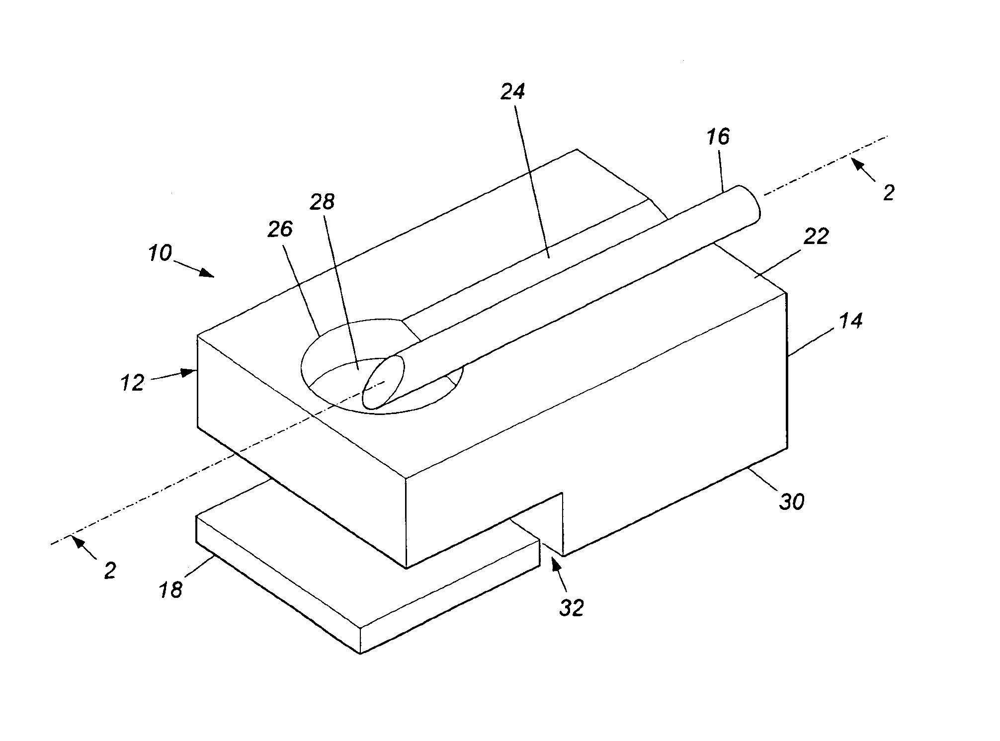
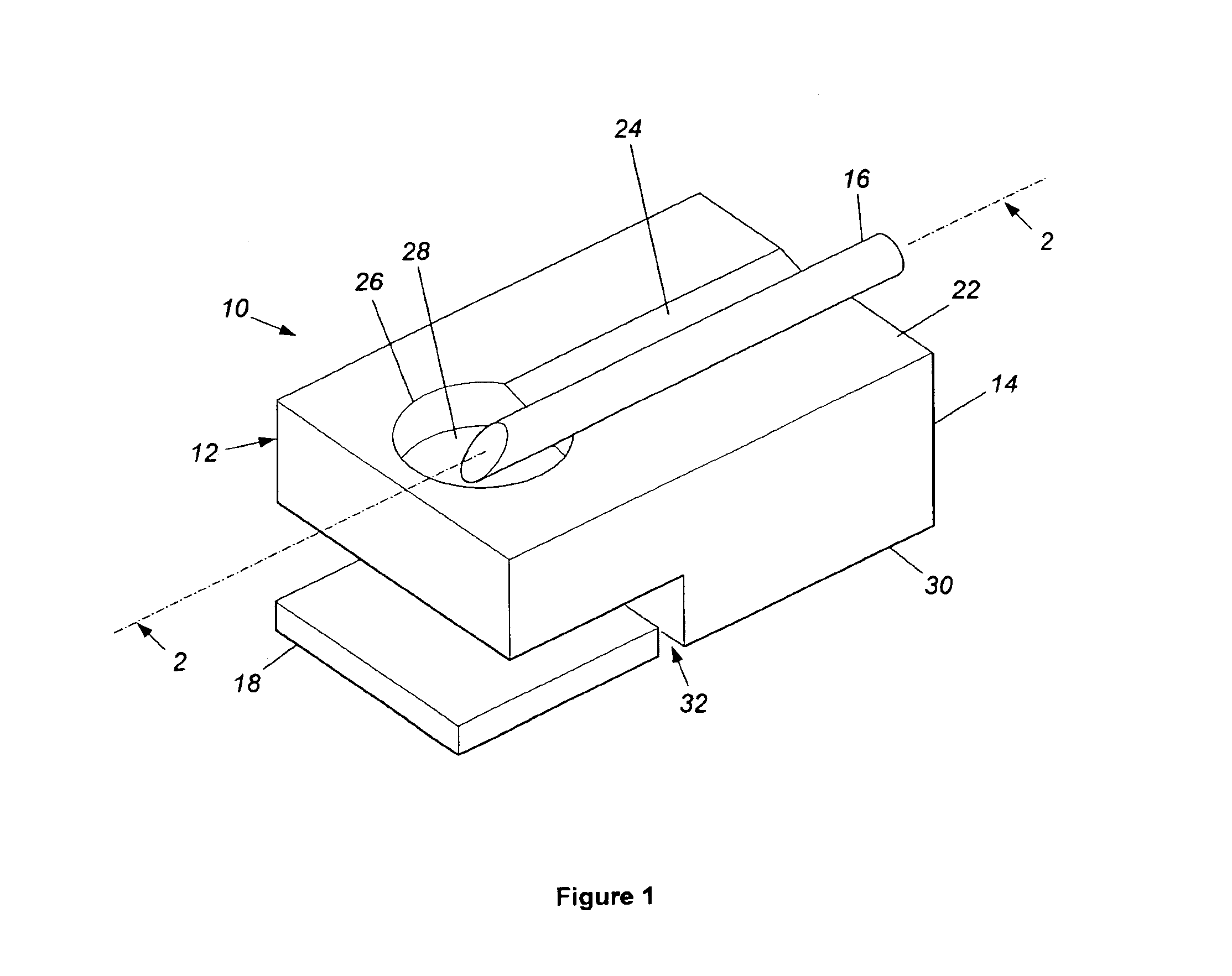
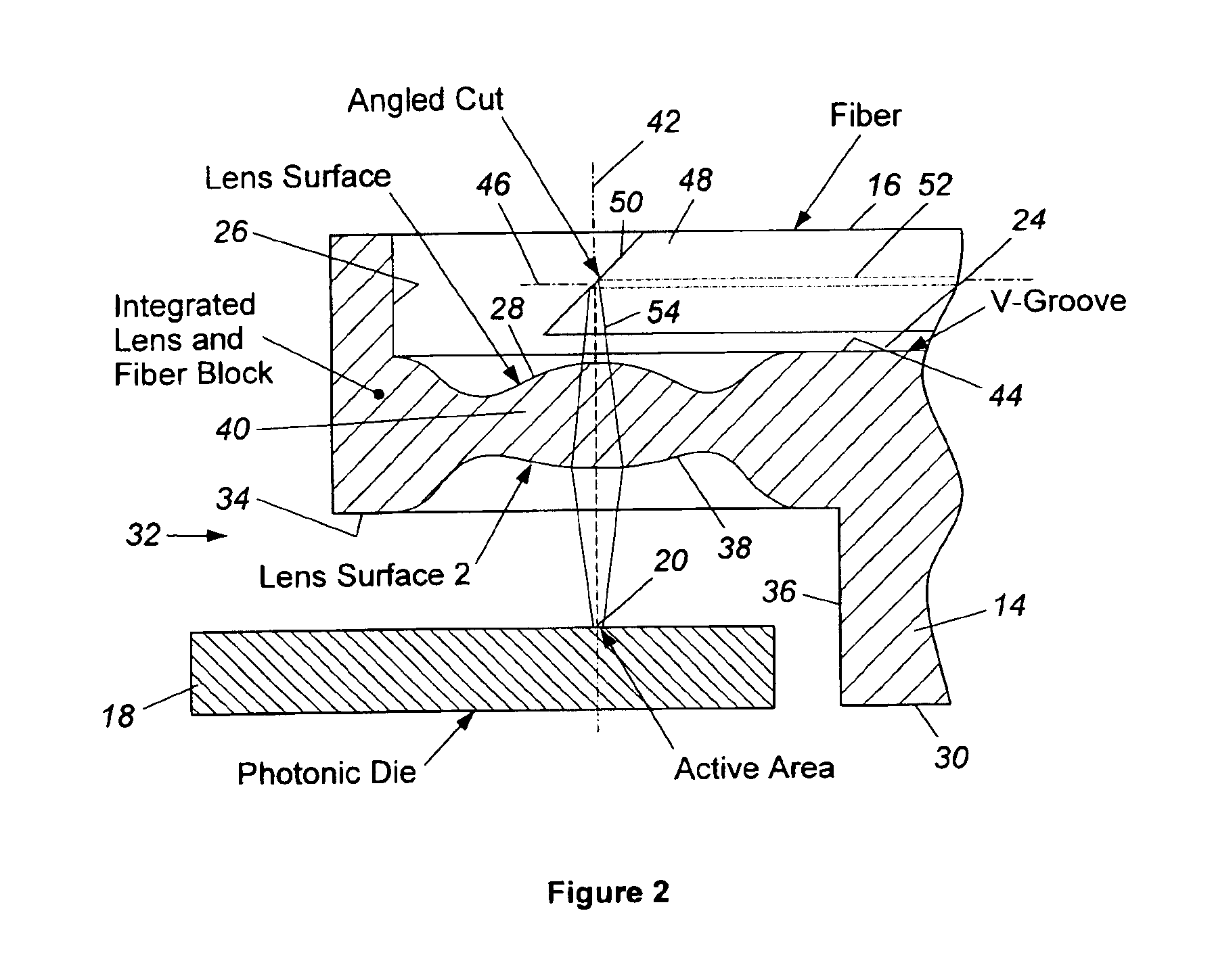
[0018]Turning now to a more detailed description of the present invention, there is illustrated in FIGS. 1, 2 and 3 a photonics package 10 which includes a semiconductor monolithic optical coupler, or alignment device 12 fabricated from a substrate 14 by a standard semiconductor etching process. This process permits fabrication of the specific features needed for the alignment device 12, as will be described below.

[0019]More specifically, the photonics package 10, which may be used, for example, in a communications or data network application for converting optical signals to corresponding electrical signals, or vice-versa, includes the alignment device 12, an optical fiber 16 supported by the alignment device, and a photonic die 18 which includes an optically active region 20, which in one embodiment may be a photodetector. In another embodiment, the region 20 may instead be a light emitter such as a VCSEL or SLED. The alignment device 12 is a monolithic structure that is created (...


PUM


Abstract

The invention relates to an optical, integrated alignment device for accurately aligning and efficiently coupling energy between in-plane optical devices. A semiconductor substrate is etched to include a groove for an optical fiber and a lens for passing an optical signal from a cut fiber to a photodetector. The etched semiconductor substrate may be used to pass an optical signal from a surface light emitting device to a cut fiber. The end of the optical fiber is cut at a slant that redirects an optical signal from the fiber through the lens or vice-versa. The lens focuses the optical signal onto a target.

Description

BACKGROUND OF THE INVENTION[0001]The present invention relates, in general, to a photonics package incorporating a monolithically integrated alignment device for coupling optical energy between in-plane optical devices and to a method for producing the same. More specifically, the invention relates to a photonics package that incorporates an optical coupling and alignment device having an integral fiber groove, lens aperture and monolithic aspheric lens.[0002]Data in optical communication systems is often transmitted in the form of optical signals through an optical fiber terminating in a photonics device such as a receiver, transponder, transceiver, or the like. The data is projected from an optical fiber, for example as a light beam, directed onto a photonic die where the data is received by a photodetector and converted to a corresponding radio frequency (RF) electrical signal. However, data can easily be lost due to improper alignment between the fiber and the photodetector or t...

Claims


Application Information

Patent Timeline
Patent Type & Authority Patents(United States)
IPC IPC(8): G02B6/42G02B6/32H01L31/0232H01S5/022
CPCG02B6/42
Inventor BROCK, JOHN C.TRAN, DEANREZEK, EDWARD A.MARQUEZ, CHRISTIAN L.HAZARD, MICHELLE M.
Owner NORTHROP GRUMMAN SYST CORP
Why Eureka
Try Eureka