Schottky barrier CMOS fabrication method

a technology of cmos and fabrication method, which is applied in the direction of semiconductor devices, electrical equipment, transistors, etc., can solve the problems of affecting the overall circuit power dissipation of most applications, affecting the overall circuit power dissipation of the circuit, and driving relatively large amounts of curren

Inactive Publication Date: 2005-12-13
AVOLARE 2 LLC
View PDF51 Cites 43 Cited by
  • Summary
  • Abstract
  • Description
  • Claims
  • Application Information

AI Technical Summary

Problems solved by technology

When ‘on’, they drive relatively large amounts of current and when turned ‘off’ they are characterized by a certain amount of leakage current.
Otherwise, the quiescent power dissipation, or the power dissipated by the CMOS circuit when idle, is a strong function of MOSFET leakage current, and significantly affects the overall circuit power dissipation for most applications.
However, leakage current increases as well.
Leaky transistors contribute to quiescent power dissipation and in extreme cases can affect the transfer of binary information during active operation.
Furthermore, depending on exactly how in the manufacturing process the channel and tailored source/drain dopants are introduced, the manufacturing cost can be affected significantly.
Another factor affecting the manufacturing cost is process yield.
The manufacturing cost of a CMOS process is a strong function of the process yield, increasing as process yield decreases.
Given traditional MOS transistor design and architecture, and CMOS manufacturing processes, there are only limited solutions to the trade-off between drive current, leakage current, parasitic capacitance and resistance, and manufacturing complexity and cost.
Previous generations of CMOS devices have relied on MOS transistors having laterally uniform, and vertically non-uniform channel doping profiles to control drain-to-source leakage currents.
However, as device channel lengths have been reduced into the 100...

Method used


Image

  • Schottky barrier CMOS fabrication method
  • Schottky barrier CMOS fabrication method
  • Schottky barrier CMOS fabrication method

Examples


Embodiment Construction

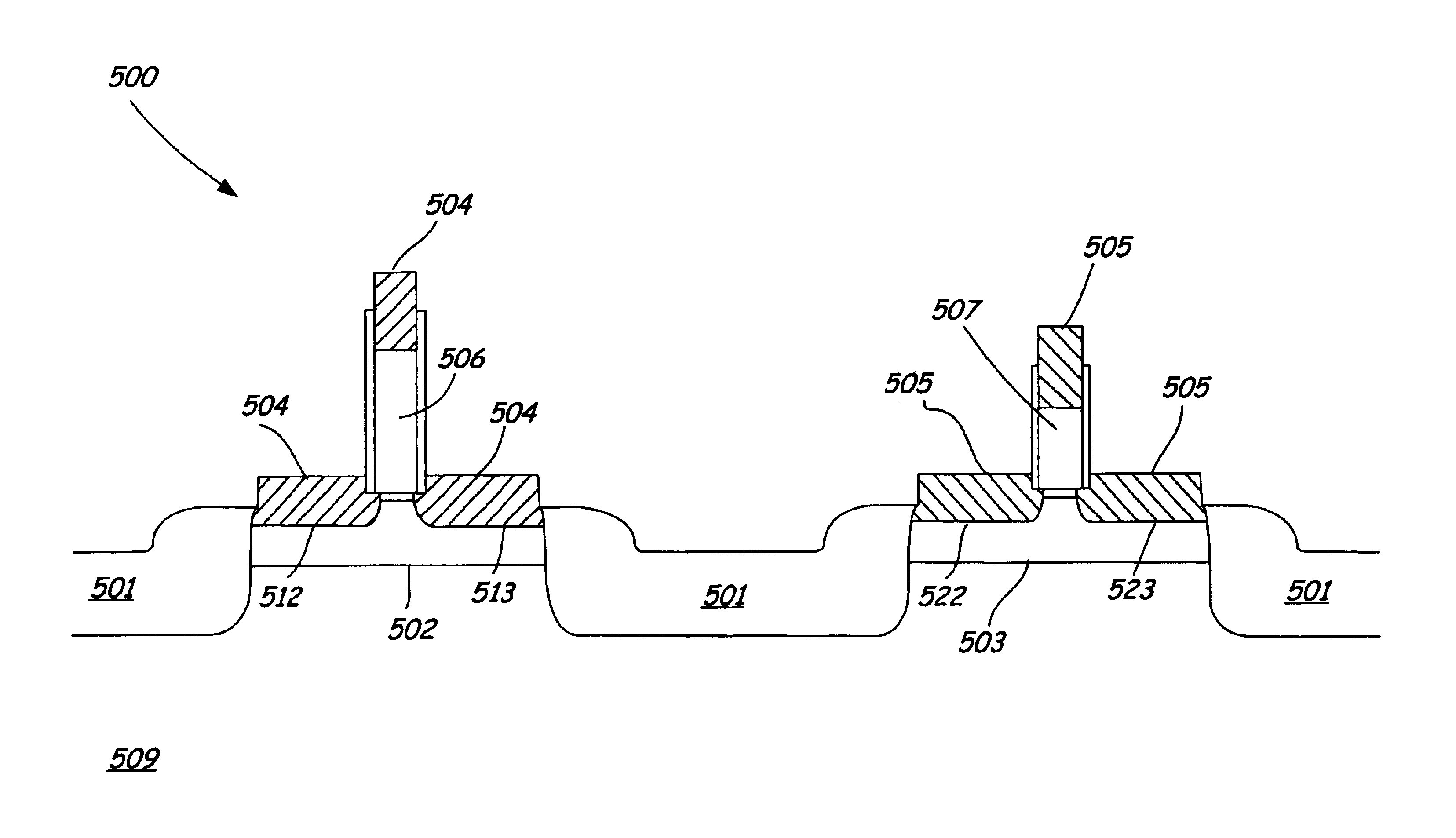
[0045]FIG. 5 shows an exemplary embodiment of the present invention, as exemplified by two final complementary MOSFET structures 500. This embodiment comprises a Schottky barrier N-channel device fabricated with Erbium Silicide 504 for the source / drain regions, and a Schottky barrier P-channel device fabricated with Platinum Silicide 505. Indium 502 and Arsenic 503 layers may be used as the channel dopants for the N-channel and P-channel devices respectively. The gate electrodes are fabricated from in-situ Phosphorous and Boron doped polysilicon films for the N-type 506 and P-type 507 devices respectively. Devices are separated from each other by a field oxide 501 that works in conjunction with the channel and substrate dopants to electrically isolate the devices from each other. The Schottky (or Schottky-like) barriers 512, 513, 522, 523) that exist along the interface of the corresponding metal source / drain 504, 505 and the silicon substrate 509 act as an inherent pocket or halo i...


PUM


Abstract

A CMOS device and method of fabrication are disclosed. The present invention utilizes Schottky barrier contacts for source and/or drain contact fabrication within the context of a CMOS device and CMOS integrated circuits, to eliminate the requirement for halo/pocket implants, shallow source/drain extensions to control short channel effects, well implant steps, and complex device isolation steps. Additionally, the present invention eliminates the parasitic bipolar gain associated with CMOS device operation, reduces manufacturing costs, tightens control of device performance parameters, and provides for superior device characteristics as compared to the prior art. The present invention, in one embodiment, uses a silicide exclusion mask process to form the dual silicide Schottky barrier source and/or drain contact for the complimentary PMOS and NMOS devices forming the CMOS device.

Description

CROSS-REFERENCE TO RELATED APPLICATION(S)[0001]This application claims priority to U.S. provisional patent application No. 60 / 445,711, filed Feb. 7, 2003. This application claims priority to U.S. provisional patent application No. 60 / 381,162, filed May 16, 2002. This application claims priority to U.S. provisional patent application No. 60 / 381,238, filed May 16, 2002. This application claims priority to U.S. provisional patent application No. 60 / 388,659, filed May 16, 2002. This application claims priority to U.S. provisional patent application No. 60 / 381,240 filed May 16, 2002. This application claims priority to U.S. provisional patent application No. 60 / 381,237, filed May 16, 2002. This application claims priority to U.S. provisional patent application No. 60 / 381,321, filed May 16, 2002. This application claims priority to U.S. provisional patent application No. 60 / 381,239, filed May 16, 2002. This application claims priority to U.S. provisional patent application No. 60 / 381,236,...

Claims


Application Information

Patent Timeline
IPC IPC(8): H01L27/095H01L29/51H01L29/78
CPCH01L27/095H01L29/7839H01L29/517
Inventor SNYDER, JOHN P.LARSON, JOHN M.
Owner AVOLARE 2 LLC
Why Eureka
Try Eureka