Copper interconnects with metal capping layer and selective copper alloys

a copper alloy and copper interconnect technology, applied in the field of copper interconnects with metal capping layers and selective copper alloys, can solve the problems of increasing the difficulty of high-performance microprocessor applications for rapid circuitry speed, more limiting circuit operating speed, cu is a mid-gap impurity in silicon, etc., to improve electromigration resistance and reduce voids in relatively narrow lines. , the effect of improving the electromigration resistan

Active Publication Date: 2005-12-27
ADVANCED MICRO DEVICES INC
View PDF1 Cites 63 Cited by
  • Summary
  • Abstract
  • Description
  • Claims
  • Application Information

AI Technical Summary

Benefits of technology

[0010]An advantage of the present invention is a method of manufacturing a semiconductor device containing Cu metallized interconnection patterns, exhibiting improved electromigration resistance in both relatively wide lines and relatively narrow lines, and having reduced voids in relatively narrow lines.
[0011]Another advantage of the present invention is a semiconductor device having Cu metallized interconnection patterns exhibiting improved electromigration resistance in both relatively wide lines and relatively narrow lines, and having reduced voids in relatively narrow lines.
[0012]Additional advantages and other features of the present invention will be set forth in the description which follows and in part will be apparent to those having ordinary skill in the art upon examination of the following or may be learned from the practice of the present invention. The advantages of the present invention may be realized and obtained as particularly pointed out in the appended claims.
[0013]According to the present invention, the foregoing and other advantages are achieved in part by a method of manufacturing a semiconductor device, the method comprising: forming a plurality of openings in a dielectric layer having an upper surface, at least one of the openings having a width no greater than a first width and at least one of the openings having a width greater than the first width; depositing a layer of substantially pure copper (Cu) or a first Cu alloy completely filling the at least one opening having a width no greater than the first width and partially filling the at least one opening having a width greater than the first width; depositing a layer of a second Cu alloy, containing an element in a sufficient amount such that the electromigration resistance along grain boundaries of the second Cu alloy is greater than that of substantially pure Cu and greater than that of the first Cu alloy, to completely fill the at least one opening having a width greater than the first width; planarizing the upper surface of the dielectric layer; forming a recess in the filled openings; and depositing a metal capping layer filling the recess.
[0014]Embodiments of the present in

Problems solved by technology

As integrated circuit geometry continues to plunge into the deep sub-micron regime, it becomes increasingly difficult to satisfy the requirements of high performance microprocessor applications for rapid circuitry speed.
The higher the value of the R×C product, the more limiting the circuit operating speed.
However, Cu is a mid-gap impurity in silicon and silicon dioxide.
Accordingly, Cu diffusion through interlayer dielectrics, such as silicon dioxide, degrades the performance of the integrate

Method used


Image

  • Copper interconnects with metal capping layer and selective copper alloys
  • Copper interconnects with metal capping layer and selective copper alloys
  • Copper interconnects with metal capping layer and selective copper alloys

Examples


Embodiment Construction

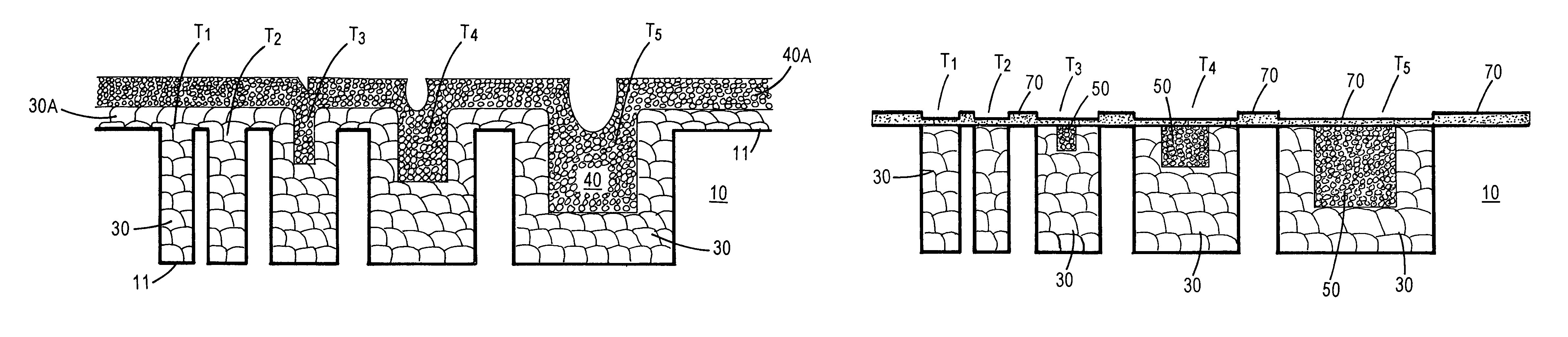
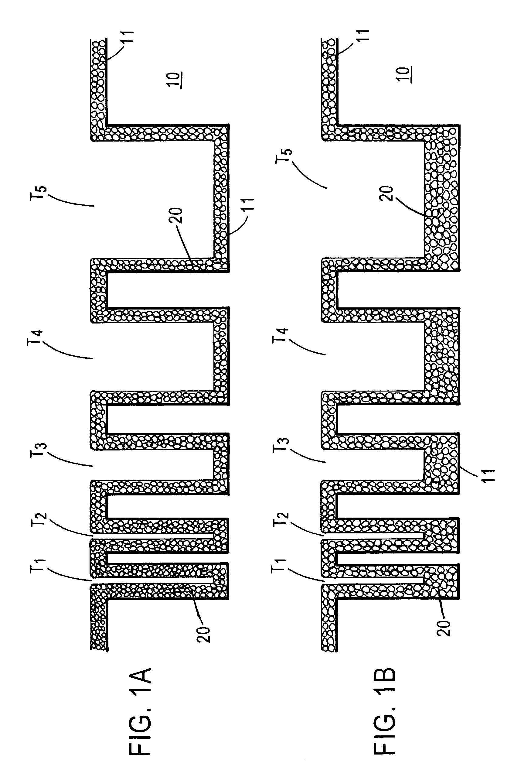
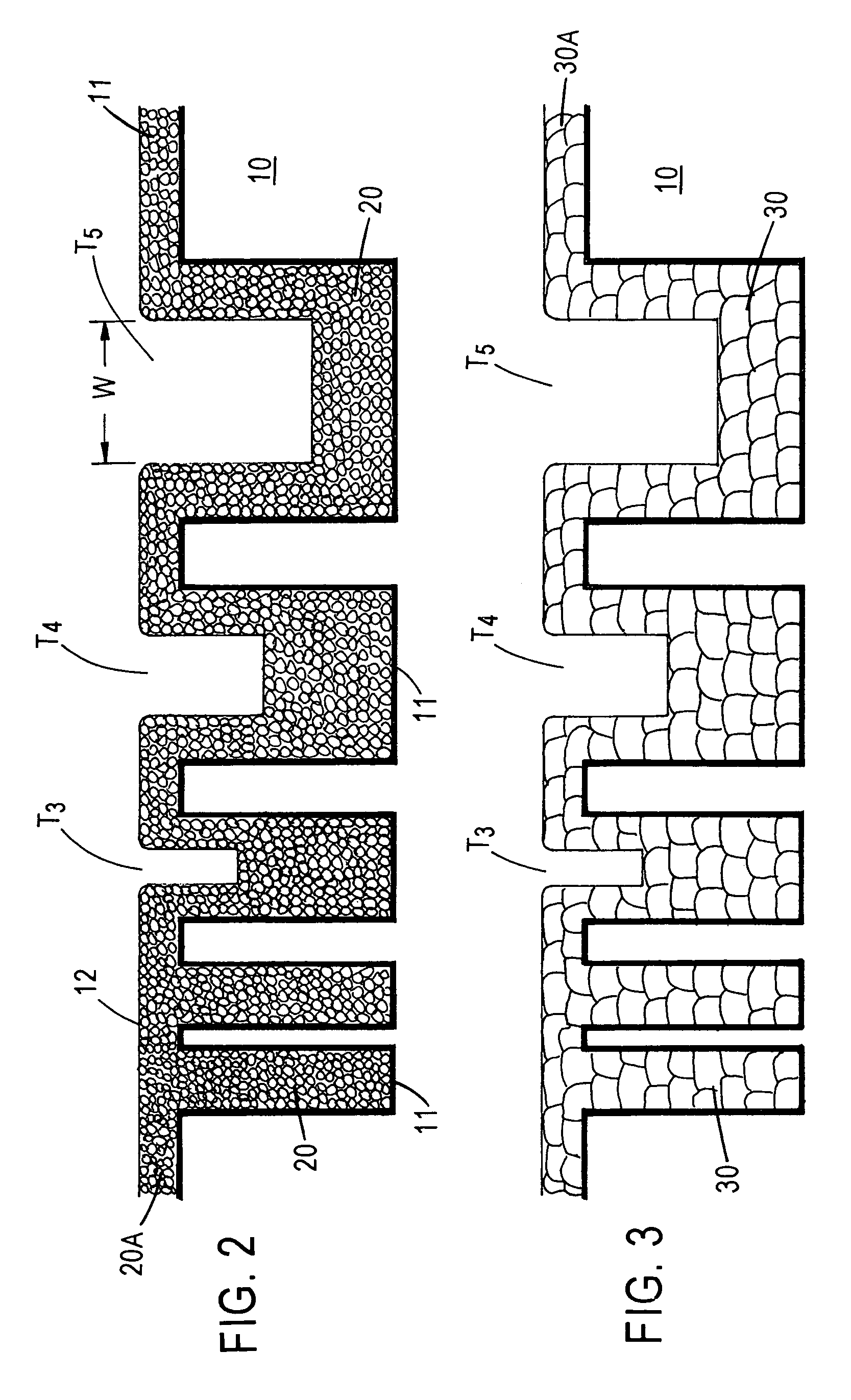
[0018]The present invention addresses and solves problems attendant upon forming Cu interconnections, particularly when implementing damascene techniques wherein Cu is deposited to fill openings in a dielectric layer that have different widths to form a metal level comprising Cu lines having different widths. Typical metal levels comprise a collection of metal lines with line widths ranging from about 1× to 50× of the smallest feature size, such as a via with a cross sectional width, e.g., a width of about 0.15 micron. Thus, in implementing damascene techniques, a plurality of openings, e.g., trenches, are formed with various size openings. Upon investigating failed or rejected semiconductor devices, it was found that the interface between the Cu metallization and capping layer, e.g., silicon nitride, is a source for electromigration failure due to Cu diffusion along the interface. In addressing this problem, substantially pure Cu was replaced with a Cu alloy containing an element, ...


PUM


Abstract

High reliable copper interconnects are formed with copper or a low resistivity copper alloy filling relatively narrow openings and partially filling relatively wider openings and a copper alloy having improved electromigration resistance selectively deposited in the relatively wider openings. The filled openings are recessed and a metal capping layer deposited followed by CMP. The metal capping layer prevents diffusion along the copper-capping layer interface while the copper alloy filling the relatively wider openings impedes electromigration along the grain boundaries.

Description

FIELD OF THE INVENTION[0001]The present invention relates to a semiconductor device comprising a highly reliable copper interconnect structure with improved electromigration resistance, and to a method of forming the highly reliable copper interconnect structure. The present invention is applicable to high speed integrated circuits, particularly integrated circuits having design features in the deep sub-micron range.BACKGROUND ART[0002]As integrated circuit geometry continues to plunge into the deep sub-micron regime, it becomes increasingly difficult to satisfy the requirements of high performance microprocessor applications for rapid circuitry speed. The speed of semiconductor circuitry varies inversely with the resistance (R) and capacitance (C) of the interconnection system. The higher the value of the R×C product, the more limiting the circuit operating speed. Miniaturization requires long interconnects having small contacts and small cross-sections. Accordingly, continuing red...

Claims


Application Information

Patent Timeline
IPC IPC(8): H01L21/3213H01L21/331H01L21/768H01L23/532
CPCH01L21/76877H01L21/76886H01L23/53238H01L21/32134H01L21/7684H01L21/76849H01L2924/0002H01L2924/00H01L21/76882
Inventor WOO, CHRISTY MEI-CHUWANG, CONNIE PIN-CHINERB, DARRELL M.
Owner ADVANCED MICRO DEVICES INC
Why Eureka
Try Eureka