Method for chemical etch control of noble metals in the presence of less noble metals

a technology of noble metals and chemical etching, applied in the field of metalurgical systems, can solve the problems of inability to easily break copper oxide films overlying metallic copper, inability to prevent the flow of thin copper(i)oxide films during the manufacturing process, and inability to reliably etch bare copper bond pads, etc., to achieve high reliability of finished ic assemblies

Active Publication Date: 2005-12-27
TEXAS INSTR INC
View PDF1 Cites 54 Cited by
  • Summary
  • Abstract
  • Description
  • Claims
  • Application Information

AI Technical Summary

Benefits of technology

[0009]Embodiments of the present invention are related to wire-bonded IC assemblies, semiconductor device packages, surface mount and chip-scale packages. It is a technical advantage that the invention offers a methodology to smooth, stable interfaces of the gold wire ball and the modified bond pad, resulting in welds with strong metallic interdiffusion. Additional technical advantages include the opportunity to scale the assembly to smaller dimensions, supporting the ongoing trend of IC miniaturization; and the absence of unwanted metals, supporting high reliability of the finished IC assemblies.

Problems solved by technology

For IC bond pads made of copper, the formation of thin copper(I)oxide films during the manufacturing process flow has to be prevented, since these films severely inhibit reliable attachment of bonding wires, especially for conventional gold-wire ball bonding.
In contrast to aluminum oxide films overlying metallic aluminum, copper oxide films overlying metallic copper cannot easily be broken by a combination of thermocompression and ultrasonic energy applied in the bonding process.
As further difficulty, bare copper bond pads are susceptible to corrosion.
This process, though, has a number of drawbacks due to technical and cost issues.

Method used


Image

  • Method for chemical etch control of noble metals in the presence of less noble metals
  • Method for chemical etch control of noble metals in the presence of less noble metals
  • Method for chemical etch control of noble metals in the presence of less noble metals

Examples


Embodiment Construction

[0025]The present invention is related to U.S. patent application Ser. No. 10 / 086,117, filed on Feb. 26, 2002 (Bojkov et al., “Waferlevel Method for Direct Bumping on Copper Pads in Integrated Circuits”).

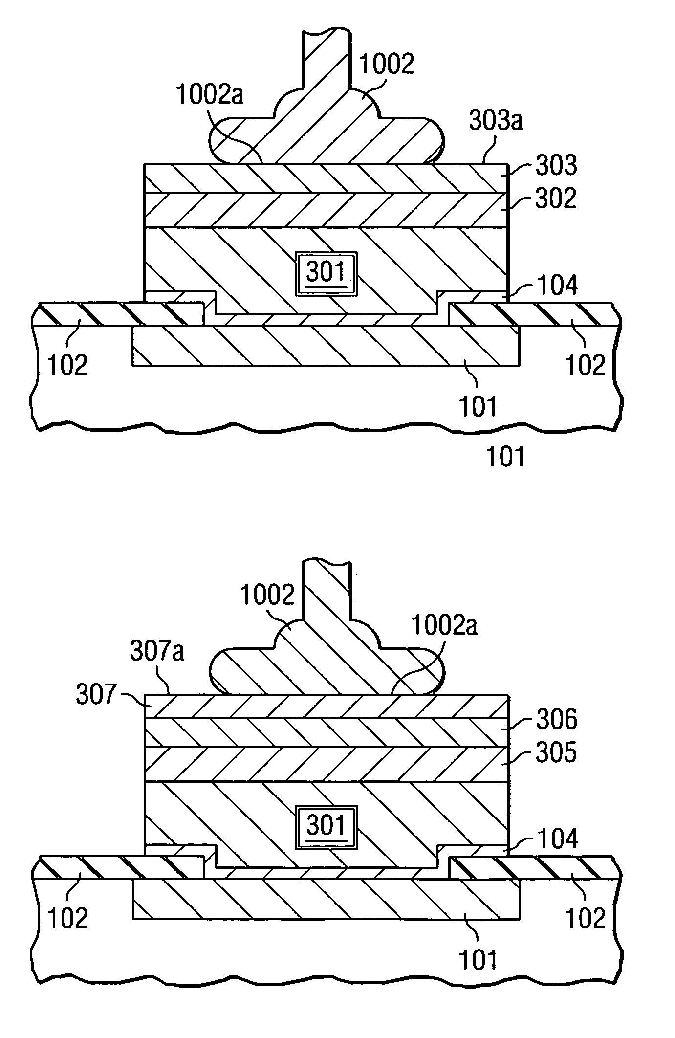
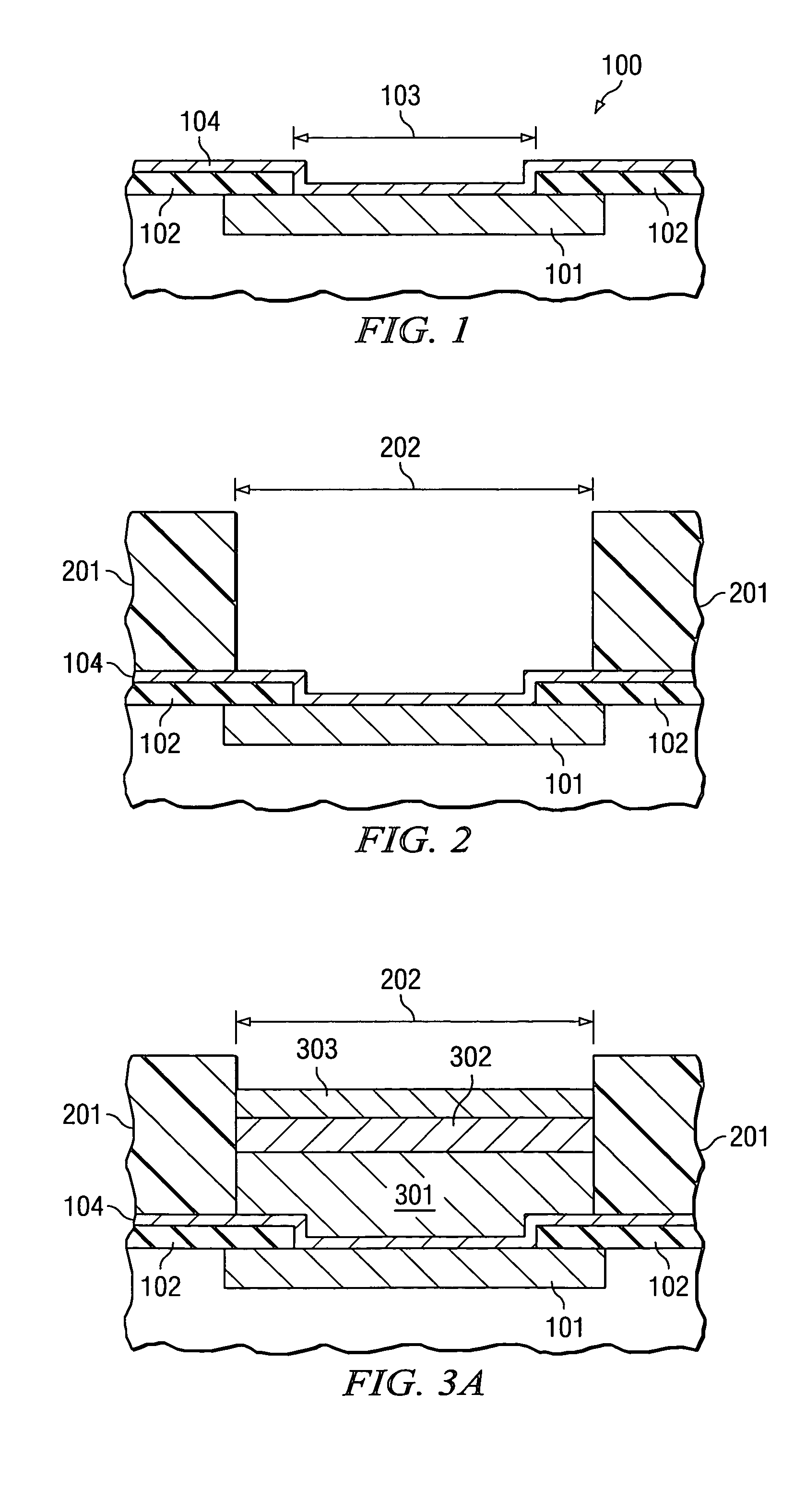
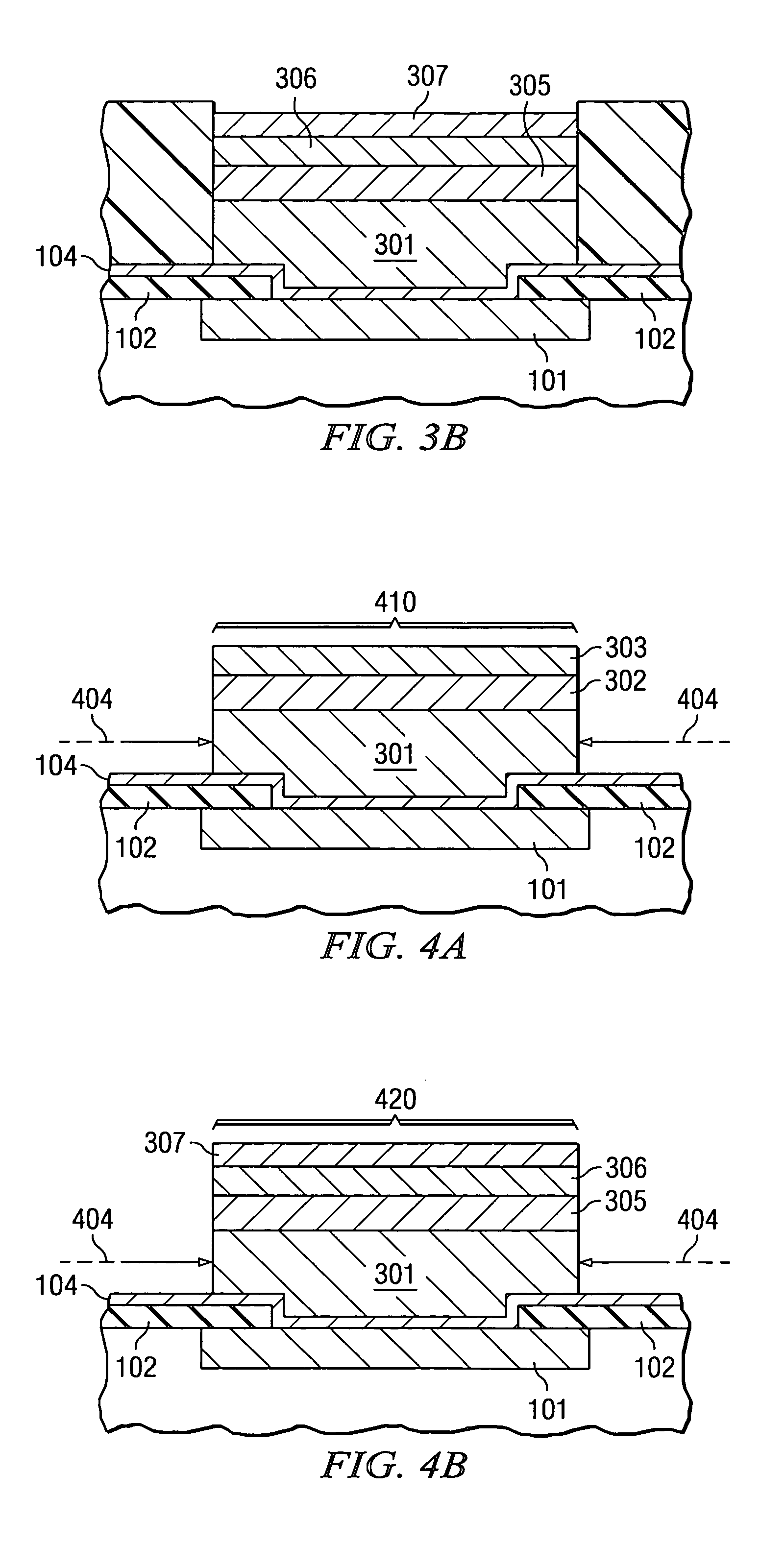
[0026]FIGS. 1 to 5B are schematic cross sections illustrating certain steps in the process flow for completing the fabrication of a bonding pad on an integrated circuit (IC) wafer. FIG. 1 shows schematically a portion of a semiconductor wafer, generally designated 100, having interconnections 101 and a protective overcoat 102. The semiconductor material is preferably silicon, but may alternatively be silicon germanium, gallium arsenide, or another III–V or II–IV semiconductor. The interconnection 101 is preferably copper; alternatively, aluminum or aluminum / copper alloy, or similar materials can be employed. The protective overcoat 102 is preferably silicon nitride, but may alternatively be silicon oxynitride, silicon carbide, silicon dioxide, or a polymer, for example. A window of ...


PUM

PropertyMeasurementUnit
thickaaaaaaaaaa
thickaaaaaaaaaa
thicknessaaaaaaaaaa

Abstract

A method for preparing a bonding pad on an integrated circuit wafer by the steps of depositing a conductive seed layer (104) on the bonding pad; depositing a metal layer (301, 302, and 303) over a portion of the conductive seed layer; and immersing the wafer in an etchant solution (501) to remove the portion of the seed layer not covered by the metal layer. The etchant solution contains a chelating agent that bonds ions from the seed layer. When the seed layer is copper or a refractory metal, and the metal layer is gold or palladium, the preferred chelating agent is selected from, but is not limited to, but is not limited to, the families of ethylenediaminetetraacetic acids (EDTA), 8-hydroxy-quinolines, including 8-hydroxy-quinoline-5-sulfonic acid, porphyrins, and phthalocyanines.

Description

FIELD OF THE INVENTION[0001]The present invention is related in general to the field of metallurgical systems with application to electronic systems and semiconductor devices and more specifically to methods of preventing unwanted depositions of less noble metals on surfaces of more noble metal during chemical etching.DESCRIPTION OF THE RELATED ART[0002]It is a continuing trend in the semiconductor industry to miniaturize integrated circuits (ICs). As a consequence of this trend, the RC time constant of the interconnection between active circuit elements increasingly dominates the achievable IC speed-power product. Consequently, there is a strong need to replace the relatively high resistivity of the interconnecting aluminum metallization by the lower resistivity of metals such as copper.[0003]For IC bond pads made of copper, the formation of thin copper(I)oxide films during the manufacturing process flow has to be prevented, since these films severely inhibit reliable attachment of...

Claims


Application Information

Patent Timeline
Patent Type & Authority Patents(United States)
IPC IPC(8): C23F1/18C23F1/30H01L21/3213H01L21/60
CPCC23F1/18C23F1/30H01L21/32134H01L24/03H01L24/05H01L24/11H01L24/48H01L24/45H01L2224/04042H01L2224/05083H01L2224/05111H01L2224/05116H01L2224/05118H01L2224/05123H01L2224/05124H01L2224/05147H01L2224/05155H01L2224/05157H01L2224/0516H01L2224/05639H01L2224/05644H01L2224/05664H01L2224/1134H01L2224/11462H01L2224/11464H01L2224/1147H01L2224/1308H01L2224/13084H01L2224/13111H01L2224/13116H01L2224/13118H01L2224/13124H01L2224/13139H01L2224/13144H01L2224/13147H01L2224/13155H01L2224/13157H01L2224/1316H01L2224/13164H01L2224/13169H01L2224/13171H01L2224/45124H01L2224/45139H01L2224/45144H01L2224/45147H01L2224/48463H01L2924/01002H01L2924/01007H01L2924/01012H01L2924/01013H01L2924/01014H01L2924/01016H01L2924/01018H01L2924/01022H01L2924/01027H01L2924/01028H01L2924/01029H01L2924/0103H01L2924/01031H01L2924/01032H01L2924/01042H01L2924/01046H01L2924/01047H01L2924/0105H01L2924/01073H01L2924/01074H01L2924/01075H01L2924/01078H01L2924/01079H01L2924/01082H01L2924/05042H01L2924/14H01L2924/3025H01L2924/00013H01L2924/01023H01L2924/01024H01L2924/01033H01L2924/01076H01L2224/48644H01L2224/48664H01L2224/48839H01L2224/48844H01L2224/48864H01L2224/48639H01L2224/48739H01L2224/48764H01L2224/0401H01L2924/00014H01L2224/13099H01L2924/00H01L2224/48744H01L2224/29099H01L2224/45014H01L2224/11901H01L2224/1146H01L2924/206H01L2224/45015H01L2924/207
Inventor BOJKOV, CHRISTO P.ARBUTHNOT, DIANE L.KUNESH, ROBERT F.
Owner TEXAS INSTR INC
Why Eureka
Try Eureka