Metal-insulator-metal capacitor and method for manufacturing the same

a technology of metal-insulator and capacitor, which is applied in the direction of capacitors, semiconductor devices, electrical equipment, etc., can solve the problems of difficult to increase the surface area of the electrode, difficult to ensure difficulty in securing the capacitance of the capacitor, so as to improve the unit capacitance improve the electrical characteristics of the mim capacitor, and prevent the generation of leakage current from the upper electrode

Active Publication Date: 2006-01-24
SAMSUNG ELECTRONICS CO LTD
View PDF27 Cites 7 Cited by
  • Summary
  • Abstract
  • Description
  • Claims
  • Application Information

AI Technical Summary

Benefits of technology

[0027]The first protection layer pattern and the second protection layer can improve the unit capacitance of the MIM capacitor because the first protection layer pattern and the second protection layer can prevent consumption of the upper electrode and the dielectric layer caused by a plasma employed in an etching process for forming the upper electrode of the MIM capacitor. Thus, the generation of leakage current from the upper electrode may be prevented while the electrical characteristics of the MIM capacitor can be improved. Additionally, because the upper electrode can be formed using the first protection layer pattern as an etching mask, the production of metallic by-products during the etching process can be prevented. Further, since the second protection layer can prevent deformation of the upper electrode, and the MIM capacitor can have a more stable structure. Furthermore, second protection layer can compensate for the consumption of the dielectric layer, thereby accomplishing subsequent processes for manufacturing the semiconductor device with enhanced stability and safety.

Problems solved by technology

As the DRAM device has been integrated to giga-grade, it has been difficult to ensure enough capacitance by varying shapes of the capacitor.
Silicon, a conventional material for the electrodes, is easily oxidized to form an interfacial oxide film at the temperature for depositing the high permittivity material, which leads to difficulty in securing the capacitance of the capacitor.
On the other hand, with the electrodes including the noble metal or the heat-resistant metal, it is difficult to increase the surface area of the electrodes, and, although the metals have excellent dielectric characteristics, their use is limited.
The heat-resistant metal electrodes have poor oxidation characteristics that further limits use of the heat-resistant metal electrodes.
In known methods for manufacturing the semiconductor device including the MIM capacitor, when the etch stop layer pattern and the upper electrode are formed using the photoresist pattern as the etch mask, the dielectric layer positioned under the upper electrode is partially removed, which can result in a failure of the capacitor.
Additionally, when the etch stop layer pattern and the upper electrode are formed using known methods, the sidewalls of the upper electrode are exposed and subject to damage that can result in the generation of a leakage current.
Further, when each structure of the MIM capacitor is formed by an etching process, the structures may be partially damaged during the etching process, resulting in an unstable MIM capacitor structure.

Method used


Image

  • Metal-insulator-metal capacitor and method for manufacturing the same
  • Metal-insulator-metal capacitor and method for manufacturing the same
  • Metal-insulator-metal capacitor and method for manufacturing the same

Examples


Embodiment Construction

[0034]Preferred embodiments of the present invention now will be described below in more detail with reference to the accompanying drawings. This invention may, however, be embodied in different forms and should not be construed as limited to the embodiments set forth herein. Rather, these embodiments are provided so that this disclosure will be thorough and complete, and will fully convey the scope of the invention to those skilled in the art. The relative thickness of layers in the illustrations may be exaggerated for purposes of describing embodiments of the present invention.

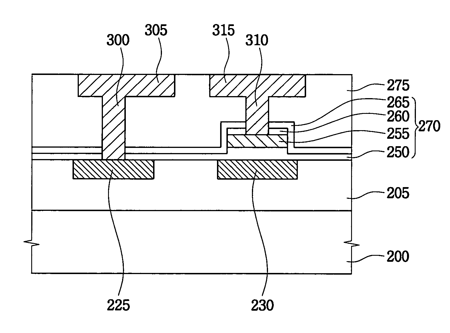
[0035]FIG. 2 is a cross-sectional view illustrating a semiconductor device including a MIM capacitor according to an embodiment of the present invention.

[0036]Referring to FIG. 2, the semiconductor device includes a MIM capacitor 140 formed on a semiconductor substrate 100 where a first insulation layer 105 and a second insulation layer 145 are formed.

[0037]The first insulation layer 105 formed on the semico...


PUM


Abstract

A capacitor has a lower electrode formed on an insulation layer, a dielectric layer formed on the lower electrode, an upper electrode layer formed on the dielectric layer, and a first protection layer pattern formed on the upper electrode layer. The upper electrode layer is etched using the first protection layer pattern to form an upper electrode. A second protection layer is formed enclosing the dielectric layer, the upper electrode and the first protection layer pattern.

Description

BACKGROUND OF THE INVENTION[0001]1. Technical Field[0002]This disclosure relates to a metal-insulator-metal (MIM) capacitor and a method for manufacturing the same. More particularly, the invention relates to a MIM capacitor including at least one protection layer to provide a stable structure and improved electrical characteristics, and a method for manufacturing the same.[0003]2. Discussion of the Related Art[0004]Known semiconductor memory devices like a dynamic random access memory (DRAM), store information like data or program commands, read the stored information and store other information. A single memory device may have one transistor and one capacitor. For example, a 16 mega-byte DRAM is a highly integrated memory device having 16 million transistors and 16 million capacitors on one chip. The capacitor in the DRAM device may include a storage node, a cell plate and an interlayer insulation layer. The capacitance of a memory device having a capacitor may be improved by enha...

Claims


Application Information

Patent Timeline
Patent Type & Authority Patents(United States)
IPC IPC(8): H01L21/20H01L27/108H01L21/02H01L21/768H01L21/8242
CPCH01L28/60H01L21/76838H01L21/76807H01L27/1085H10B12/03H10B12/00
Inventor PARK, SANG-HOON
Owner SAMSUNG ELECTRONICS CO LTD
Why Eureka
Try Eureka