

Surface emitting semiconductor laser and manufacturing method thereof
a surface-emitting semiconductor and laser technology, applied in laser cooling arrangements, laser details, optical resonator shape and construction, etc., can solve the problems of high threshold current, difficult to increase the optical output power of the device to a range of several mw to several tens mw, and unsuitable for consumer goods, etc., to achieve high output power, low resistance, and high efficiency
- Summary
- Abstract
- Description
- Claims
- Application Information
AI Technical Summary
Benefits of technology
Problems solved by technology
Method used
Image

Examples
first embodiment
(First Embodiment)
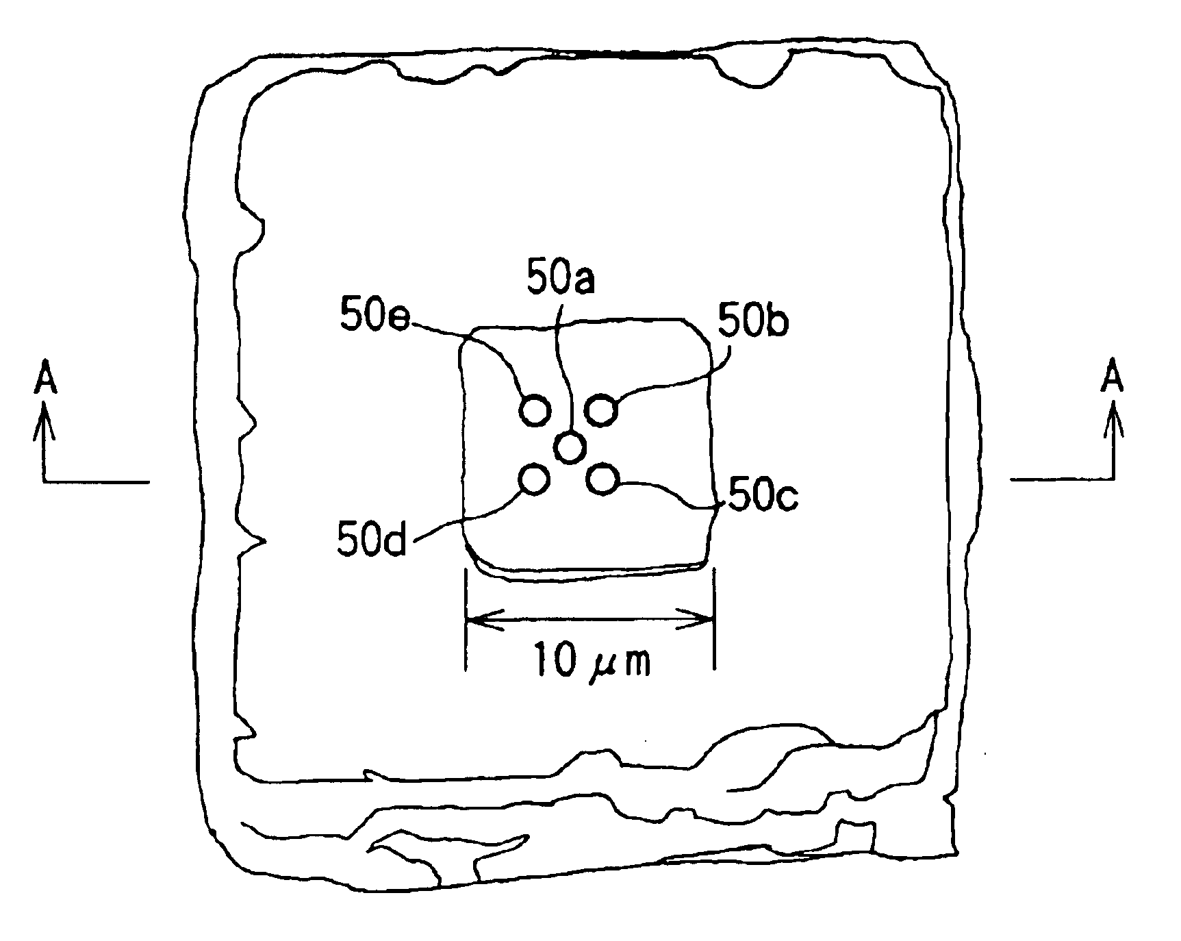
[0086]In the first embodiment, a surface emitting semiconductor laser provided with the boundary region of a spot etching type and a manufacturing method thereof will be described. The method of the present embodiment corresponds to the method of manufacturing a surface emitting semiconductor laser of the eleventh aspect of the present invention.
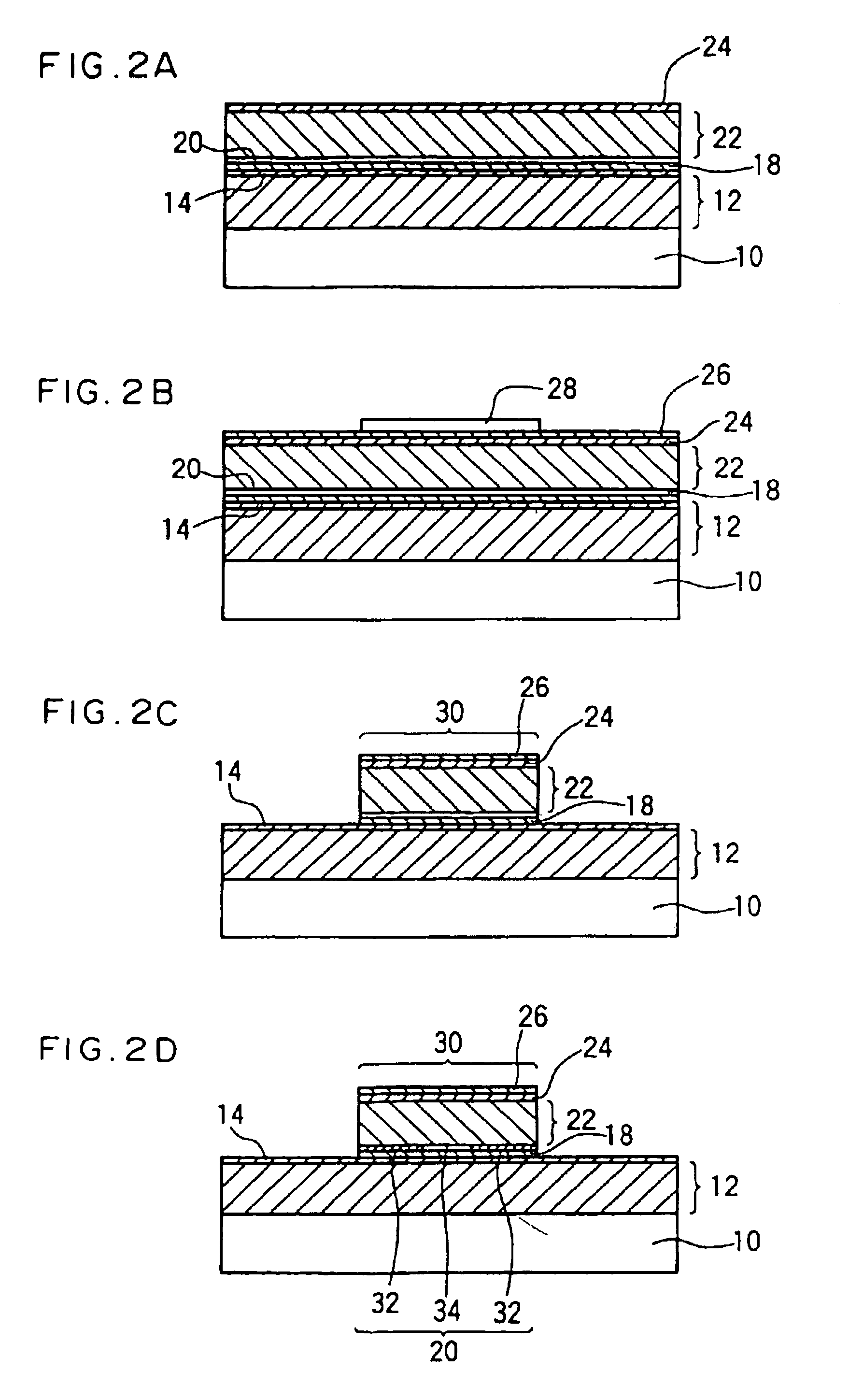
[0087]First, as shown in FIG. 2A, a lower multilayer reflection film 12 formed of a plurality of laminated bodies each of which is formed of a pair of n-type Al0.8Ga0.2As layer and n-type Al0.1Ga0.9As layer, a lower spacer layer 14 formed of an undoped Al0.4Ga0.6As layer, a quantum well active layer (not shown) formed of a laminated body of a quantum well layer formed of an undoped GaAs layer and a barrier layer formed of an undoped Al0.2Ga0.8As layer, an upper spacer layer 18 formed of an undoped Al0.4Ga0.6As layer, a p-type AlAs layer 20, an upper multilayer reflection film 22 formed of a plurality of laminated bodies eac...
second embodiment
(Second Embodiment)
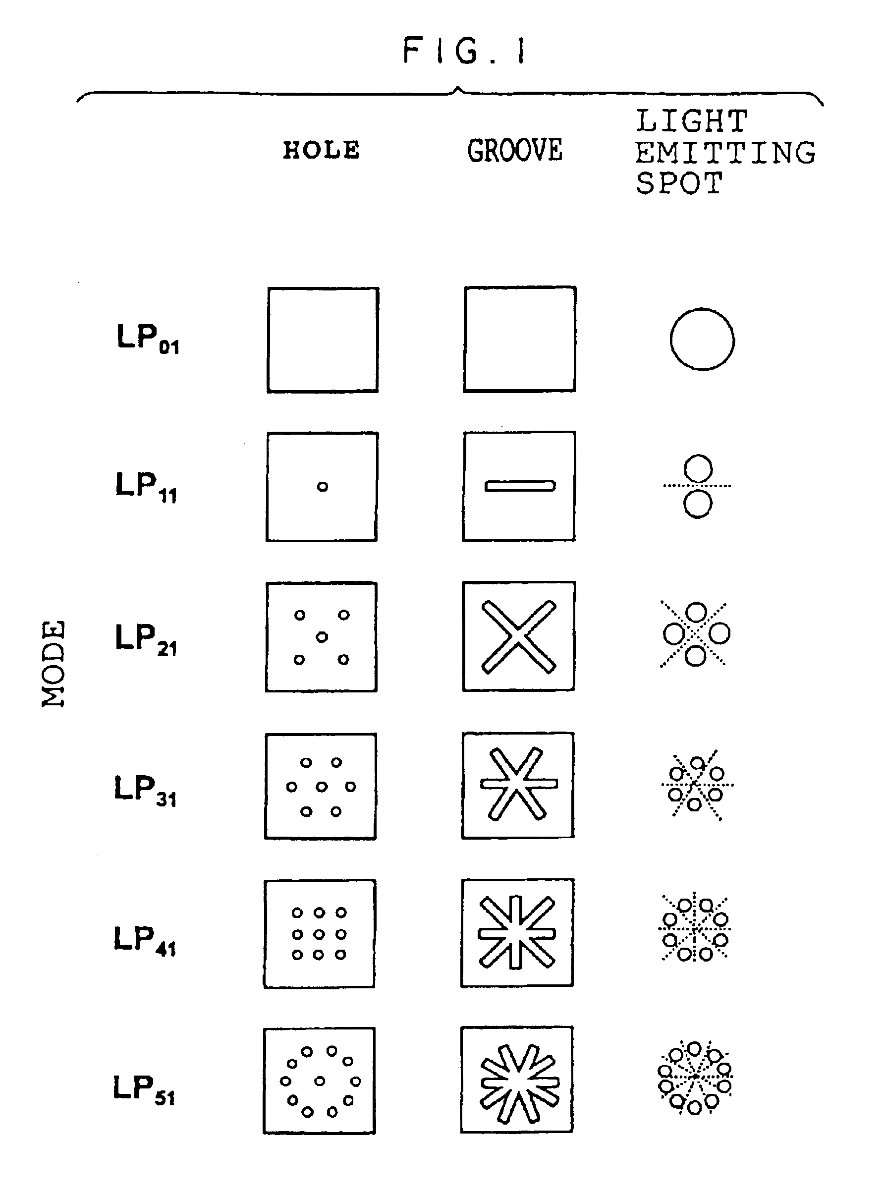
[0107]While spot etching for forming the circular holes of a small diameter was performed on the surface of the multilayer reflection film to form the recesses for suppressing the light emission of oscillation mode except for the specific oscillation mode in the first embodiment described above, a stripe etching for forming narrow grooves as the recesses to produce the same effect is performed in the present second embodiment. Here, since the longitudinal (lamination) structure of the substrate and manufacturing processes except for the surface processing in the second embodiment are the same as those in the first embodiment, their description will be omitted and description will be made only for the different parts. Further, the method of the present second embodiment corresponds to the method for manufacturing the surface emitting semiconductor laser of the twelfth aspect of the present invention.
[0108]Following the process shown in FIG. 2F in the first embodime...
third embodiment
(Third Embodiment)
[0114]The third embodiment is a modification of the first embodiment and the second embodiment described above, and is different in the longitudinal (lamination) structure of the substrate from the first and second embodiments. That is, the upper multilayer reflection film is formed of a Ga0.5In0.5P layer 33 in place of the Al0.8Ga0.2As layer. Since the other portions in the present embodiment are the same as those in the first two embodiments, like reference symbols in the first embodiment are assigned to the parts similar or corresponding to those in the first embodiment and their description will be omitted. Here, the Ga0.5In0.5P layer 33 corresponds to the etching preventing layer of the present invention and the method of the present embodiment corresponds to the method of manufacturing the surface emitting semiconductor laser of the twelfth aspect of the present invention.
[0115]In FIG. 12A, a lower multilayer reflection film 12 formed of a plurality of lamina...
PUM
 Abstract
Description
Claims
Application Information