Method and apparatus for forming improved metal interconnects

Inactive Publication Date: 2006-01-31
APPLIED MATERIALS INC
View PDF100 Cites 35 Cited by
  • Summary
  • Abstract
  • Description
  • Claims
  • Application Information

AI Technical Summary

Benefits of technology

[0013]Following sputter-etching, the second copper layer is deposited over the barrier layer and the exposed first copper layer to complete copper interconnect formation. Because the first and second copper layers are in direct contact, the high resistivity of the barrier layer is eliminated. Accordingly, the inventive copper interconnect has low resistance in addition to no via-to-via leakage current paths.
[0014]In a second aspect, a capping dielectric barrier layer (e.g., silicon nitride) is deposited over the first copper layer prior to interlayer dielectric formation. Preferably, the capping dielectric barrier layer is deposited before the first copper layer is exposed to oxygen (e.g., air) to prevent copper oxide formation on the first copper layer. Thereafter, the capping dielectric barrier layer and any copper oxide formed on the first copper layer are sputter-etched. Because the capping dielectric barrier layer is sp

Problems solved by technology

Unlike aluminum, however, copper is highly mobile in silicon dioxide and may, as a result of infiltration of copper atoms into the dielectric, create leakage paths through a device's various dielectric layers.
Copper atoms also can cause electrical defects in silicon.
Such deleterious via-to-via leakage currents, however, cannot be avoided in conventional copper interconnects if the copper oxide layer 1

Method used


Image

  • Method and apparatus for forming improved metal interconnects
  • Method and apparatus for forming improved metal interconnects
  • Method and apparatus for forming improved metal interconnects

Examples


Embodiment Construction

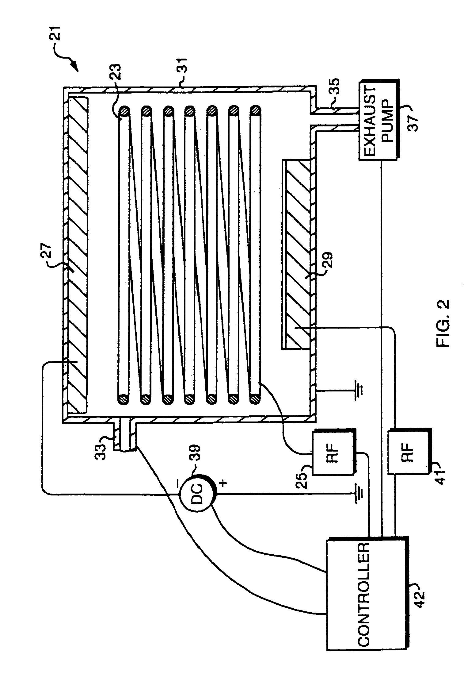
[0030]In the preferred aspects of the present invention, copper interconnect formation is performed primarily within a high density plasma sputtering chamber (although interconnect vias may be filled by a process for filling vias, such as chemical vapor deposition (CVD), physical vapor deposition (PVD) or electroplating as is known in the art). Accordingly, before discussing the preferred aspects for copper interconnect formation, the operation of such a high density plasma sputtering chamber is described briefly with reference to FIG. 2.

[0031]FIG. 2 is a side diagrammatic illustration, in section, of the pertinent portions of a high density plasma sputtering chamber 21 for practicing the present invention. The sputtering chamber 21 contains a wire coil 23 which is operatively coupled to a first RF power supply 25. The wire coil 23 may comprise a plurality of coils, a single turn coil as shown in FIG. 2, a single turn material strip, or any other similar configuration. As shown in F...


PUM


Abstract

Methods of forming copper interconnects free from via-to-via leakage currents and having low resistances are disclosed. In a first aspect, a barrier layer is deposited on the first metal layer prior to copper oxide sputter-etching to prevent copper atoms from reaching the interlayer dielectric and forming via-to-via leakage current paths therein. In a second aspect, a capping dielectric barrier layer is deposited over the first metal layer prior to sputter etching. During sputter-etching, the capping dielectric barrier layer redistributes on the sidewalls of the interlayer dielectric, preventing sputter-etched copper atoms from reaching the interlayer dielectric and forming via-to-via leakage paths therein. In a third aspect, both a capping dielectric barrier layer and a barrier layer are deposited over the first metal layer prior to sputter-etching to prevent copper atoms produced during sputter-etching from reaching the interlayer dielectric and forming via-to-via leakage paths therein.

Description

[0001]This application is a continuation of U.S. patent application Ser. No. 10 / 067,709, filed Feb. 5, 2002 now U.S. Pat. No. 6,709,987 , which is a continuation of U.S. Ser. No. 09 / 928,891 filed Aug. 13, 2001, now U.S. Pat. No. 6,559,061, which is a continuation of U.S. Ser. No. 09 / 126,890, filed Jul. 31, 1998, now U.S. Pat. No. 6,287,977, all of which are hereby incorporated by reference herein in their entirety.FIELD OF THE INVENTION[0002]The present invention relates to semiconductor device metal layer interconnects and more particularly to reducing the contact resistance of interconnects.BACKGROUND OF THE INVENTION[0003]A typical integrated circuit contains a plurality of metal pathways to provide electrical power for powering the various semiconductor devices comprising the integrated circuit, and to allow these semiconductor devices to share / exchange electrical information. Within integrated circuits, metal layers are stacked on top of one another by using intermetal or “inte...

Claims


Application Information

Patent Timeline
IPC IPC(8): H01L21/302H01L21/285H01L21/28H01L21/768H01L23/522H01L23/532
CPCH01L21/76805H01L21/76814H01L21/76831H01L21/76834H01L21/76838H01L21/76844H01L21/76877H01L23/5226H01L23/53238H01L2924/0002H01L2924/00
Inventor HASHIM, IMRANCHIANG, TONYCHIN, BARRY
Owner APPLIED MATERIALS INC
Why Eureka
Try Eureka