

Wafer planarization composition and method of use
a technology of semiconductor wafers and compositions, applied in the direction of grinding machines, manufacturing tools, aqueous dispersions, etc., can solve problems such as scratches on the wafer surface, and achieve the effect of increasing the cut rate and enhancing the performance of chemical mechanical planarization processes
Inactive Publication Date: 2006-02-14
3M INNOVATIVE PROPERTIES CO
View PDF25 Cites 13 Cited by
- Summary
- Abstract
- Description
- Claims
- Application Information
AI Technical Summary
Benefits of technology
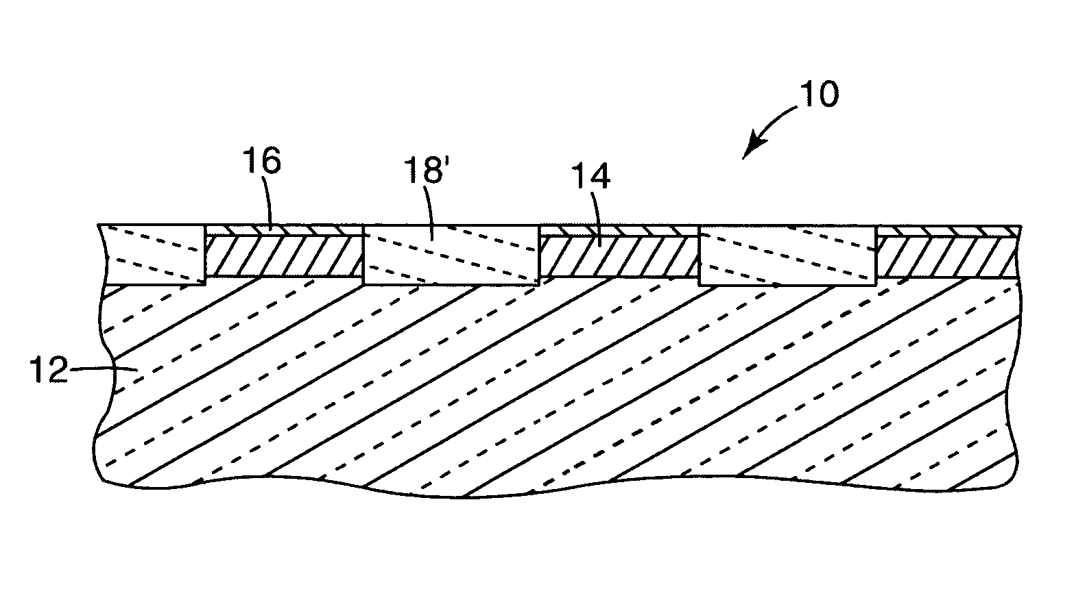
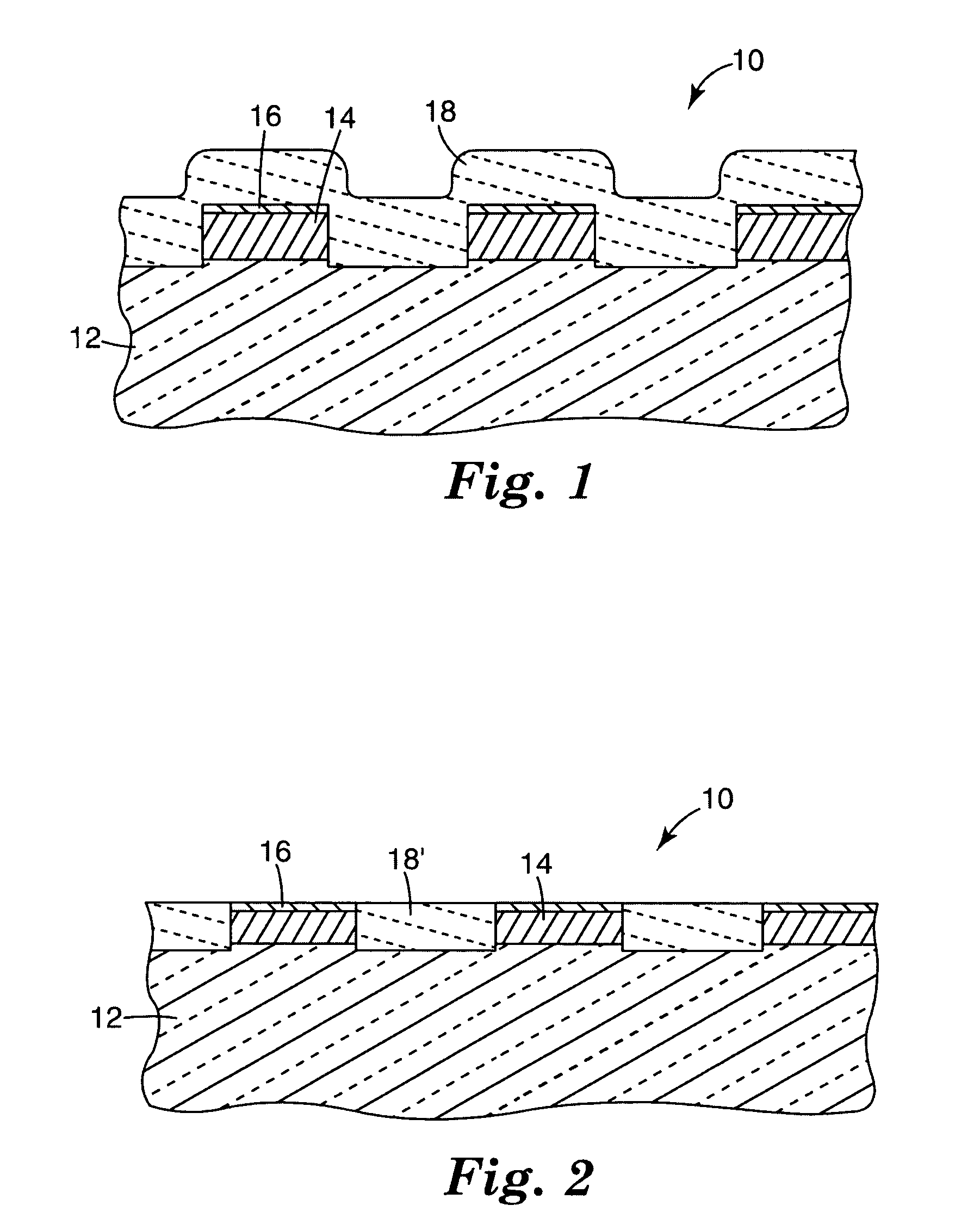
The present invention provides a composition for modifying the surface of a semiconductor wafer during chemical mechanical planarization processes. The composition can be adjusted to control cut rate and selectivity for modifying the wafer using a fixed abrasive CMP process. The use of a three-dimensional, textured, fixed abrasive article with abrasive particles and a binder increases the cut rate while retaining selectivity for removing silicon dioxide and silicon nitride. The composition can also include a working liquid with at least one amino acid and calcium or barium ions. The invention enhances the performance of chemical mechanical planarization processes and provides a better surface quality for semiconductor wafers.
Problems solved by technology
Flocculated slurry particles may lead to scratches on the wafer surface.
Method used
View moreImage
Smart ImageViewing Examples

Examples
examples
[0048]The salts in the following examples are calcium chloride (CaCl2), calcium hydroxide (Ca(OH)2), barium hydroxide octahydrate (Ba(OH)2•8H2O), aluminum chloride (AlCl3), sodium chloride (NaCl), and magnesium chloride hexahydrate (MgCl2•6H2O) (all available from Alfa-Aesar, Ward Hill, Mass.). The material designations shown in TABLE 1 are used throughout the examples.
[0049]
TABLE 1DesignationMaterialCACLcalcium chloride (CaCl2)CAOHcalcium hydroxide (Ca(OH)2)BAOHbarium hydroxide octahydrate (Ba(OH)2)ALCLaluminum chloride (AlCl3)NACLsodium chloride (NaCl)MGCLmagnesium chloride hexahydrate (MgCl2.6H2O)AA1L-prolineAA2L-histidine
Login to View More PUM
| Property | Measurement | Unit |
|---|---|---|
| diameter | aaaaa | aaaaa |
| diameter | aaaaa | aaaaa |
| surface speed | aaaaa | aaaaa |
Abstract
Description
FIELD OF INVENTION[0001]The present invention relates generally to a composition for modifying an exposed surface of a semiconductor wafer. More particularly, the present invention relates to a composition that can be adjusted to control cut rate and selectivity for modifying semiconductor wafers using a fixed abrasive chemical-mechanical planarization process.BACKGROUND[0002]During integrated circuit manufacture, semiconductor wafers used in semiconductor fabrication typically undergo numerous processing steps, including deposition, patterning, and etching steps. Details of these manufacturing steps for semiconductor wafers are reported by Tonshoff et al., “Abrasive Machining of Silicon”, published in the Annals of the International Institution for Production Engineering Research, (Volume 39 / 2 / 1990), pp. 621–635. In each manufacturing step, it is often necessary or desirable to modify or refine an exposed surface of the wafer in order to prepare the wafer for subsequent fabrication...
Claims
Login to View More Application Information
Patent Timeline
 Patent Type & AuthorityPatents(United States)
IPC IPC(8): B24B1/00
CPCC09G1/04H01L21/31053
InventorRUEB, CHRISTOPHER J.WEBB, RICHARD J.VELAMAKANNI, BHASKAR V.
Owner3M INNOVATIVE PROPERTIES CO