Semiconductor device configured for suppressed germanium diffusion from a germanium-doped regions and a method for fabrication thereof

Inactive Publication Date: 2006-03-07
TRECENTI TECHNOLOGIES INC +1
View PDF7 Cites 11 Cited by
  • Summary
  • Abstract
  • Description
  • Claims
  • Application Information

AI Technical Summary

Benefits of technology

[0019]With any one of the forms stated above, it is possible to provide a high-performance and low-resistance semiconductor device capable of suppressing leakage currents. This in turn makes it possible to constitute a semiconductor device with high reliability for offering enhanced suppressibility of changes in characteristics such as threshold voltage values of transistors used.
[0020]Additionally, in an exemplary semiconductor device having at least one of the gate electrode and the channel underlayer film made of silicon germanium as their main component material, it is possible to offer at least one of the effects which follow. For example, it

Problems solved by technology

The influence given to signal transmission delay by an increase in resistance resulted from a decrease in line width of gate electrode—this has not specifically been considered as a serious problem in past days—is becoming more significant to an extent that such is no longer negligible for achievement of ultrahigh-speed transistor operations.
One of recently challenged approaches to discovery of such material satisfying the above-noted requirements is to make use of silicon germanium for gate electrodes.
This is relied upon the fact that giving such strain to the silicon underlying a gate dielectric film results in an increase in electron mobility.
Unfortunately, since metal oxide semiconductor (MOS) transistor microfabrication processes typically require addition of thermal processing steps at high temperatures after having fabricated gate electrodes and/or channel underlayer films, the gate electrodes and ch

Method used


Image

  • Semiconductor device configured for suppressed germanium diffusion from a germanium-doped regions and a method for fabrication thereof
  • Semiconductor device configured for suppressed germanium diffusion from a germanium-doped regions and a method for fabrication thereof
  • Semiconductor device configured for suppressed germanium diffusion from a germanium-doped regions and a method for fabrication thereof

Examples


first embodiment

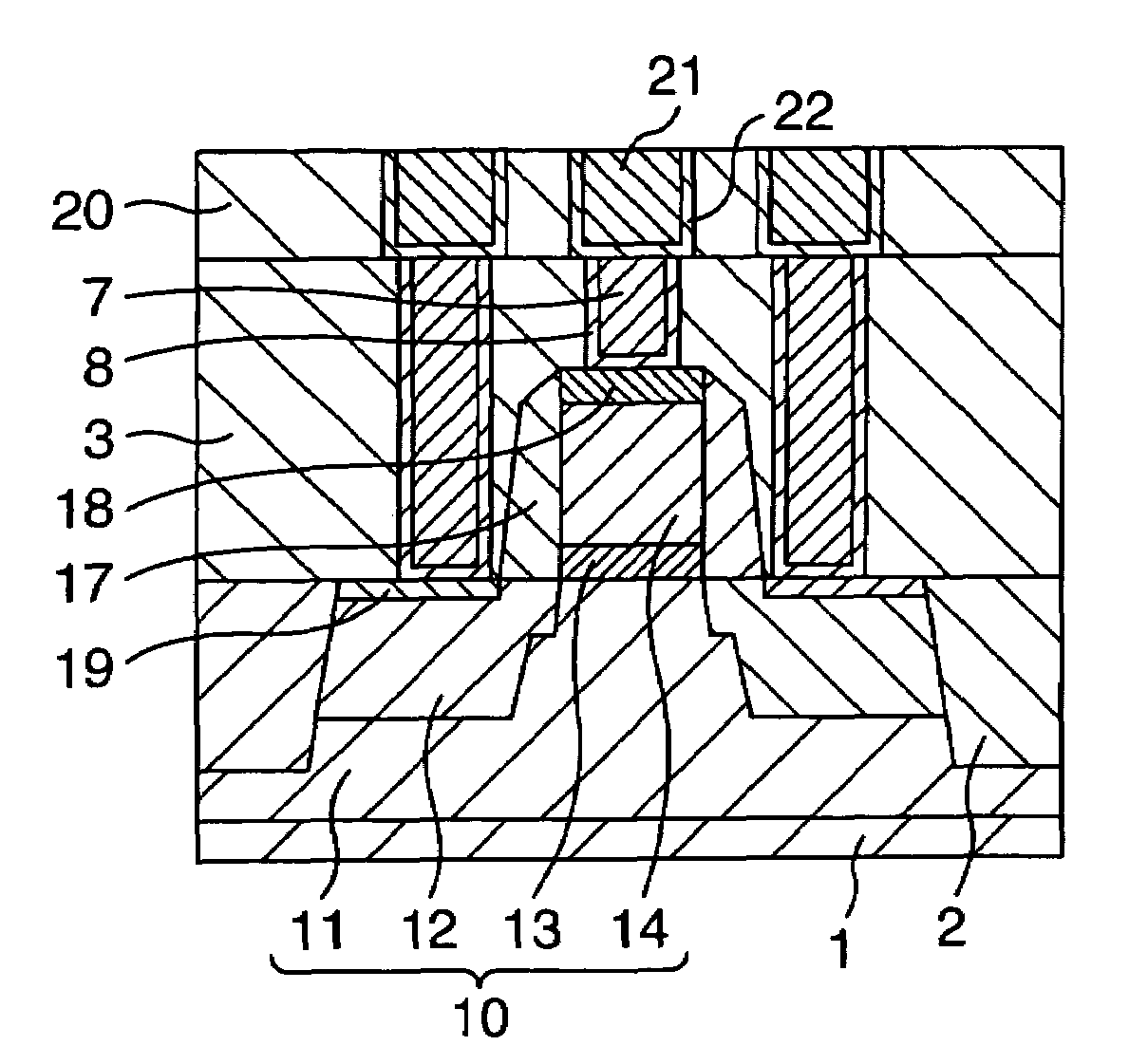
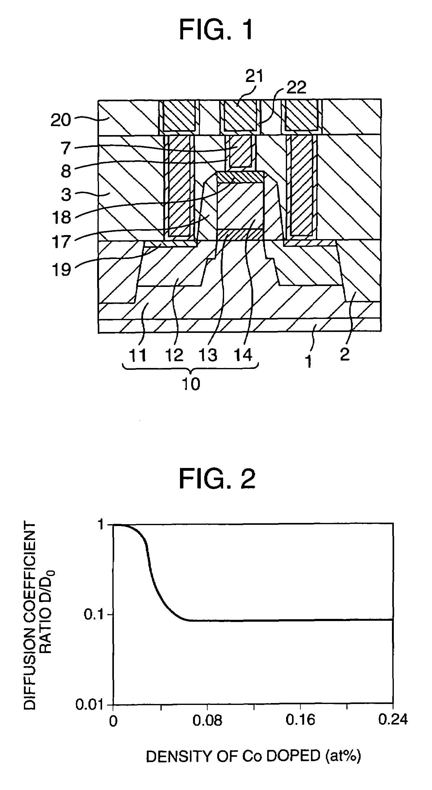
[0035]A cross-sectional structure of main part of a semiconductor device in accordance with a first embodiment of the invention is shown in FIG. 1. As shown in FIG. 1, the semiconductor device of this embodiment is structured from a field effect transistor 10, which is formed on a silicon substrate 1.

[0036]The field effect transistor 10 includes a pair of spaced-apart source / drain regions 12 formed in a well 11, a gate dielectric film 13, and a gate electrode 14. The gate electrode 14 has its upper surface on which a silicide film 18 is formed, whereas the source / drain 12 has its surface on which a silicide 19 is formed. Note that the source / drain 12 refers to either a source region or a drain region, wherein these source / drain regions laterally oppose each other with the overlying gate electrode 14 residing therebetween. A difference between the source and the drain is principally originated from the difference in direction of current flow. As these regions are similar to each othe...

second embodiment

[0063]A cross-sectional structure of main part of a semiconductor device in accordance with a second embodiment of this invention is shown in FIG. 8. A principal difference of the second embodiment from the first embodiment is that the gate electrode has a two-layer structure consisting essentially of a first gate electrode 14a and a second gate electrode 14b. Regarding the remaining parts or components, the second embodiment is similar in structure to the first embodiment. Silicon germanium is used for the second gate electrode 14b as its main component material, which electrode 14b is arranged to contain Co or N as doped thereinto to a concentration similar to that of the gate electrode 14 of the first embodiment stated supra. Alternatively the gate electrode 14b is designed to contain C at a concentration similar to that of the gate electrode 14 of first embodiment. The first gate electrode 14a is made of either silicon or silicon germanium as its main constituent material. Note ...

third embodiment

[0064]A sectional structure of main part of a semiconductor device which is a third embodiment of the invention is shown in FIG. 9A. A main difference of the third embodiment over the first embodiment lies in that the gate electrode has a three-layer structure consisting essentially of a first gate electrode 14a, a second gate electrode 14b and a third gate electrode 14c. The third embodiment is similar to the first embodiment in structures of the other parts. Silicon germanium is used as the main component material of the first gate electrode 14a, second gate electrode 14b and third gate electrode 14c. The second gate electrode 14b is arranged to contain either Co or N, which is doped to a concentration similar to that of the gate electrode 14 of the first embodiment. Alternatively let it contain C as its doping atoms at a concentration similar to that of the gate electrode 14 of first embodiment. As shown in FIG. 9B, the first gate electrode 14a contains Co or N as its doped atoms...


PUM


Abstract

In semiconductor devices, a semiconductor device is provided which is high in reliability while suppressing changes in characteristics such as threshold voltages. In a semiconductor device which has a gate dielectric film above a semiconductor substrate and also has above the gate dielectric film a gate electrode film made of silicon germanium chosen as its main constituent material, or alternatively in a semiconductor device which has beneath the gate dielectric film a channel made of silicon as its main constituent material and which has below the channel a channel underlayer film made of silicon germanium as its main constituent material, a specifically chosen dopant, such as cobalt (Co) or carbon (C) or nitrogen (N), is added to the gate electrode and the channel underlayer film, for use as the unit for suppressing diffusion of germanium in the gate electrode or in the channel underlayer film.

Description

BACKGROUND OF THE INVENTION[0001]1. Field of the Invention[0002]The present invention relates to semiconductor devices.[0003]2. Description of the Prior Art[0004]In recent years, with advances in information communication equipment, semiconductor devices such as large-scale integrated (LSI) circuit chips are becoming more strict year by year in processing performance required therefore. Under the circumstances, attempts are made to speed up the operating rates of transistors. Until today, such speed-up of transistor operation has been advanced mainly based on miniaturization or shrinkage of the fabrication sizes of gate electrodes. Recently, the gate length is shrunk to 0.1 micrometer (μm) or less. Another requirement is that the film thickness of a gate electrode is much reduced to about 20 nanometers (nm) in cases where silicon is used as the main constituent material thereof. The influence given to signal transmission delay by an increase in resistance resulted from a decrease in...

Claims


Application Information

Patent Timeline
IPC IPC(8): H01L31/117H01L29/423H01L21/28H01L21/331H01L21/336H01L29/10H01L29/167H01L29/49H01L29/732H01L29/737H01L29/78H01L29/786
CPCH01L21/2807H01L29/1004H01L29/7378H01L29/167H01L29/4966H01L29/1054B41F16/0086B41F16/0093
Inventor NASU, SHINGOIWASAKI, TOMIOOHTA, HIROYUKIKUMAGAI, YUKIHIROIKEDA, SHUJI
Owner TRECENTI TECHNOLOGIES INC
Why Eureka
Try Eureka