Measuring chip

a technology of measuring chip and dielectric block, which is applied in the direction of color/spectral property measurement, phase-affecting property measurement, instruments, etc., can solve the problems of discontinuous refractive index, difficult operation of uniting the two dielectric blocks into an integral body, and uneven so as to reduce the degree of depolarization of linearly polarized light, less fluctuation, and good reproducibility

Inactive Publication Date: 2006-03-07
FUJIFILM CORP +1
View PDF5 Cites 1 Cited by
  • Summary
  • Abstract
  • Description
  • Claims
  • Application Information

AI Technical Summary

Benefits of technology

[0055]The inventors have found that a fluctuation in measured data in the measuring chip for surface plasmon resonance measurement or leaky mode measurement is practically negligible if the state of polarization immediately before the measuring chip is kept about 50%, and is almost negligible if it is kept about 90% (i.e., if the degree of depolarization is about 10% or less). FIG. 6 shows the relationship between the photoelastic coefficient of the material (resin) of a dielectric block and the degree of depolarization of the linearly polarized light passed through the dielectric body. It can be seen from the figure that when the photoelastic coefficient is 50×10−12 Pa−1 and 20×10−12 Pa−1, the degree of depolarization is the above-described values, that is, 50% and 10%. Hence, in the present invention, the photoelastic coefficient of the material of the dielectric block is less than 50×10−12 Pa−1, preferably less than 20×10−12 Pa−1. Therefore, in the measuring chip of the present invention, the degree of depolarization of linearly polarized light can be reduced, and measured data with less fluctuation and good reproducibility can be obtained.
[0056]In the measuring chip of the present invention, the film layer (metal film, etc.,) that is formed on one surface of the dielectric block is usually formed by vapor deposition. If the percentage of water absorption of the dielectric body is higher when vapor deposition is performed, then the time required for deaerating the vapor deposition device up to a vacuum state will become longer. FIG. 7 is a graph showing the relationship between the percentage of water absorption of the material of a dielectric block and the deaerating time required in vapor-depositing a metal film on the dielectric block (time required to deaerate the vapor deposition device up to 4×10⁻¹² Pa−1). As shown in the figure, if the percentage of water absorption is less than 0.2%, the above-described deaerating time is reduced to less than 20 min which is practically allowable in almost all cases, and the time required for vapor deposition can be shortened.
[0057]Note that if the percentage of the material (resin) of the dielectric block is great, the dielectric body will absorb the water in a sample during measurement and therefore the refractive index will change greatly. If the refractive index of the dielectric body changes greatly in this way, the angle at which attenuated total reflection (ATR) takes place will fluctuate regardless of the dielectric constant or refractive index of a sample to be measured. Therefore, if a resin whose percentage of water absorption is low is employed as the material of the dielectric body, a fluctuation in measured data due to the moisture absorption of the dielectric block can be reduced.

Problems solved by technology

However, in the case where the conventional measuring chip which is exchangeable is employed, a gap occurs between the first dielectric block and the second dielectric block and the refractive index becomes discontinuous.
The operation of uniting the two dielectric blocks into an integral body is fairly difficult, and consequently, the conventional measuring chip is not easy to handle in making a measurement.
In such a case, the loading and removal of the measuring chips are time-consuming.
As a result, the efficiency of the automatic measurement is reduced.
In addition, there is a possibility that the conventional measuring chip will have a detrimental influence on the environment, because it uses an index-matching solution.
However, in a conventional measuring chip equipped with such a resin dielectric block, there are cases where the reproducibility of measured data is not good.

Method used


Image

  • Measuring chip
  • Measuring chip
  • Measuring chip

Examples


first embodiment

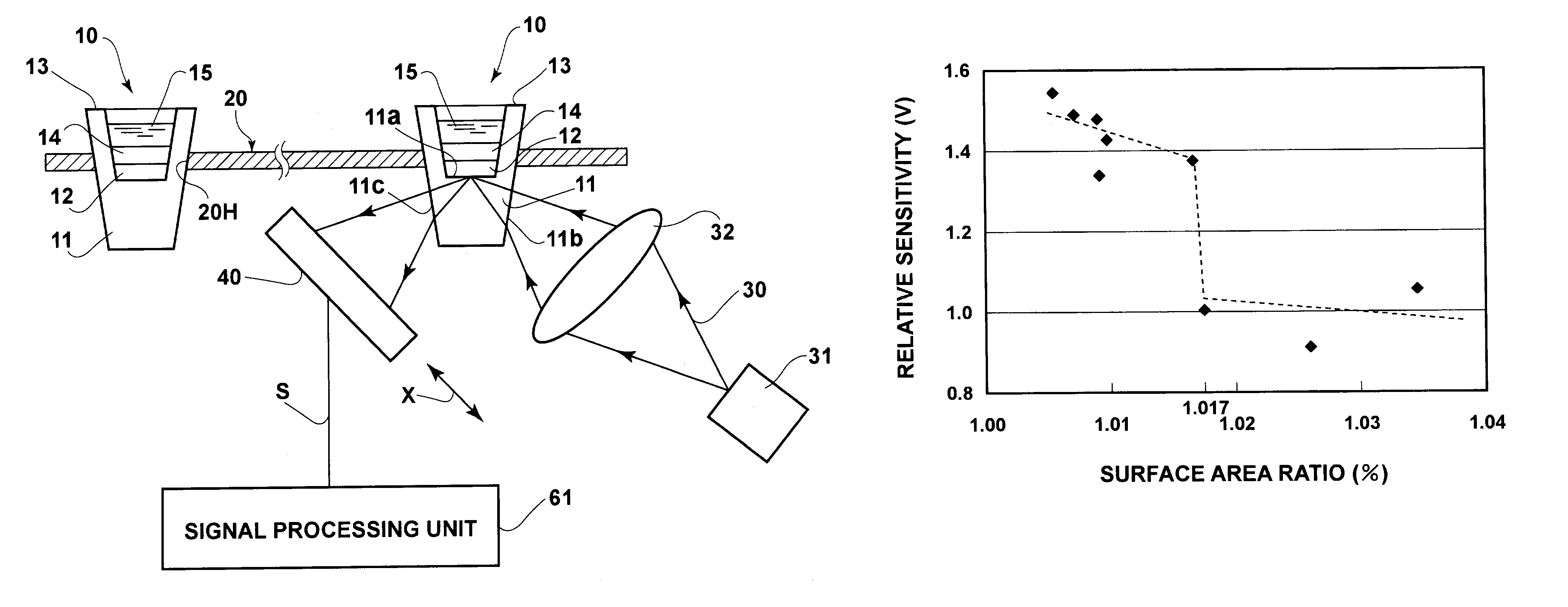
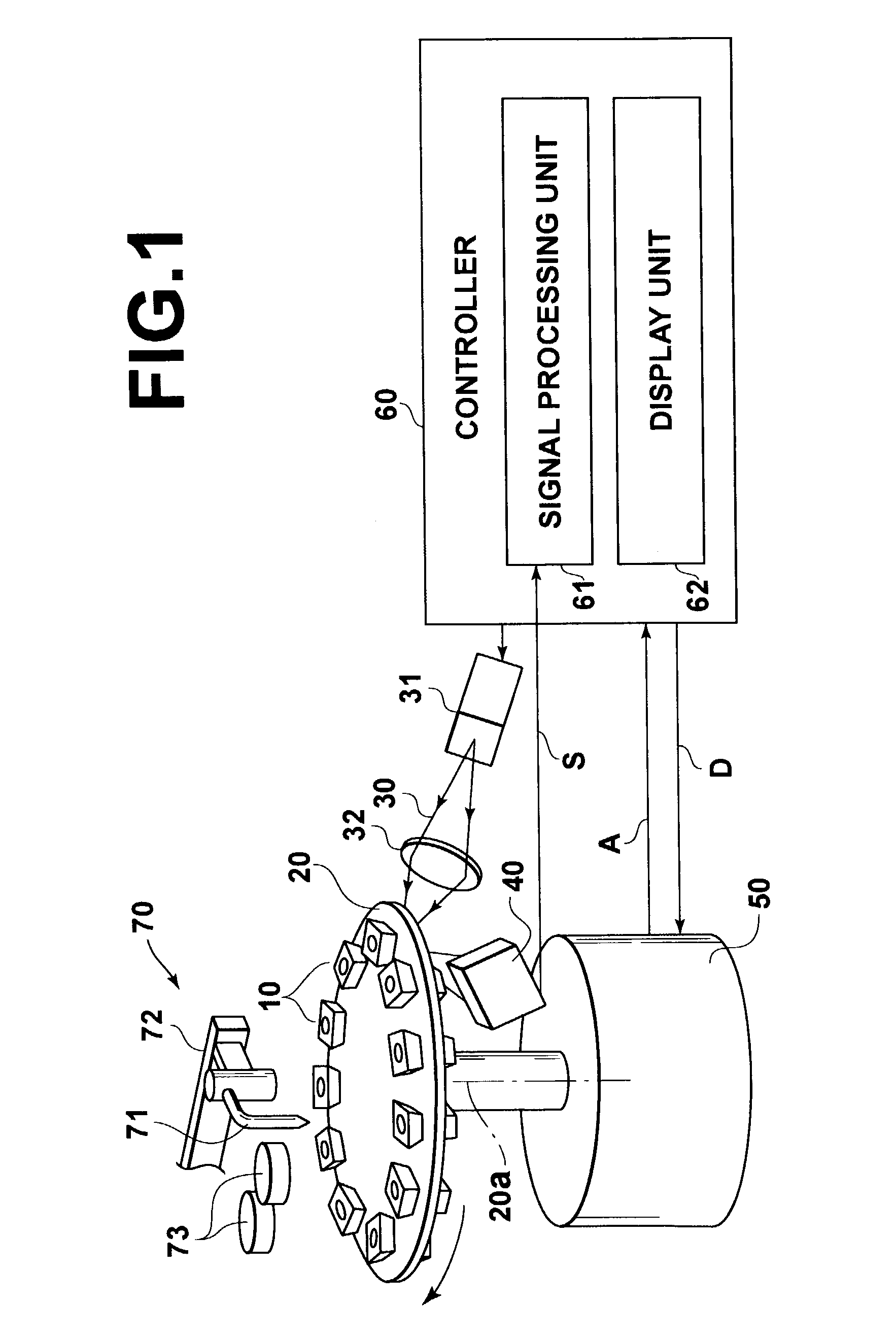
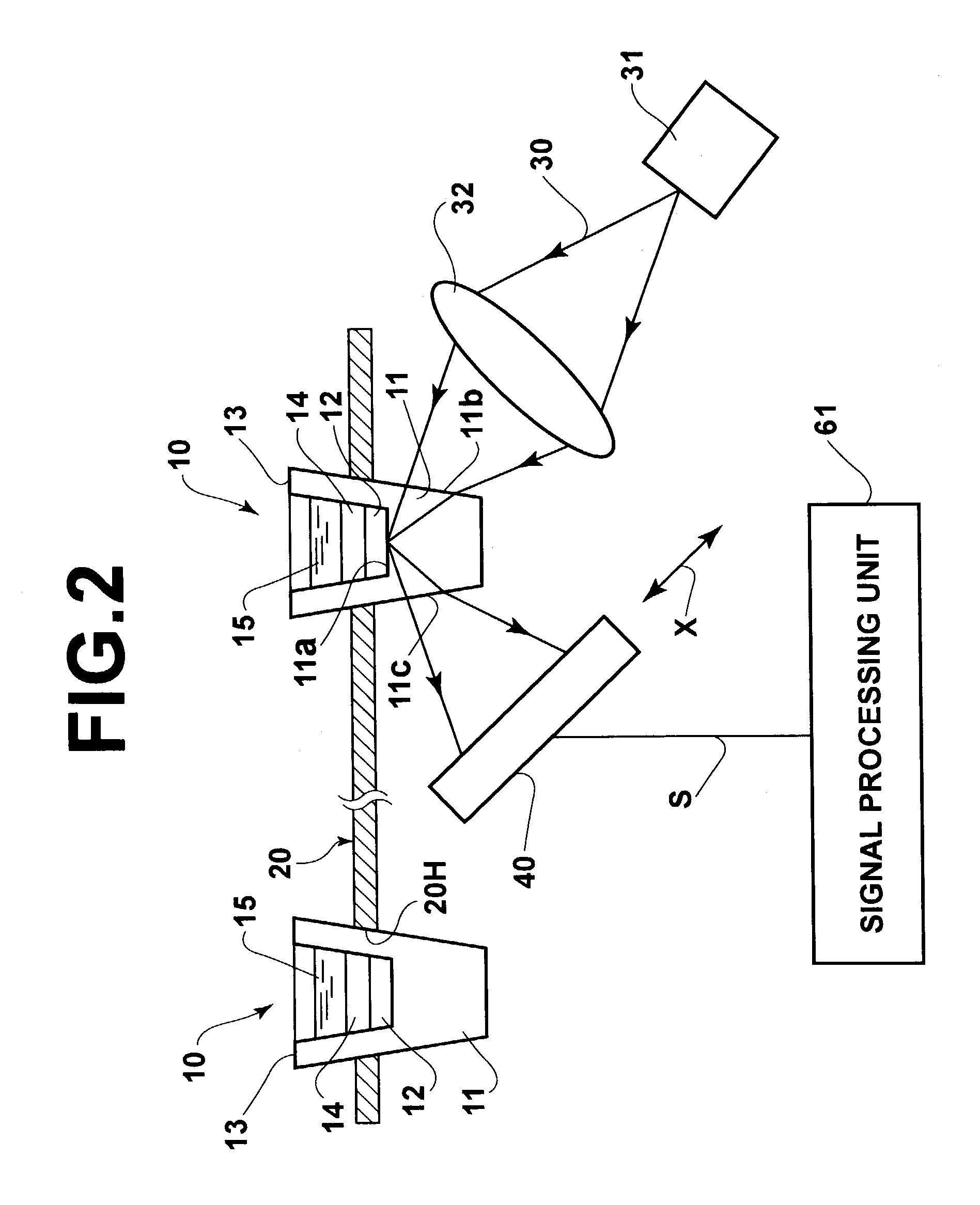
[0069]Referring now in greater detail to the drawings and initially to FIG. 1, there is shown a surface plasmon resonance measurement apparatus which employs surface plasmon resonance measuring chips (hereinafter referred to simply as measuring chips) 10 constructed in accordance with the present invention.

[0070]As illustrated in FIG. 1, the surface plasmon resonance measurement apparatus has a turntable 20 for supporting a plurality of measuring chips 10. The apparatus also has a laser light source (e.g., a semiconductor laser) 31 for emitting a measuring light beam (e.g., a laser beam) 30, a condenser lens 32 constituting an optical incidence system, and a photodetector 40. The apparatus further has supporting-body drive means 50 for rotating the turntable 20 intermittently, a controller 60, and an automatic sample supply mechanism 70. The controller 60 controls the supporting-body drive means 50, and also performs a process described later in response to a signal S from the photo...

second embodiment

[0094]Referring now to FIG. 5, there is shown a leaky mode measurement apparatus that employs measuring chips 700 constructed in accordance with the present invention. The leaky mode measurement apparatus is basically the same in construction as the surface plasmon resonance measurement apparatus shown in FIG. 2. The measuring chip 700 includes a cladding layer 701 formed on one surface (e.g., the top surface) of a dielectric body 11, and an optical waveguide layer 702 formed on the cladding layer 701.

[0095]The dielectric block 11 is injection-molded by employing, for example, the aforementioned resin, “ZEONEX 330R.” The cladding layer 701 is formed into the shape of a thin film by employing a dielectric or metal (such as gold, etc.) lower in refractive index than the dielectric block 11. The optical waveguide layer 702 is also formed into a thin film by employing a dielectric which is higher in refractive index than the cladding layer 701. The film thickness of the cladding layer 7...


PUM

PropertyMeasurementUnit
water absorptionaaaaaaaaaa
widthaaaaaaaaaa

Abstract

A measuring chip comprising a dielectric block and a thin film layer formed on one surface of the dielectric block. The thin film layer is used for placing a sample thereon. The dielectric block is formed as a single block, which includes an entrance surface at which a light beam enters the dielectric block, an exit surface from which the light beam emerges, and the one surface on which the thin film layer is formed. In addition, the dielectric block is integrated with the thin film layer and formed from a resin whose photoelastic coefficient is less than 50×10−12 Pa−1.

Description

BACKGROUND OF THE INVENTION[0001]1. Field of the Invention[0002]The present invention relates to a measuring chip that is employed in a surface plasmon resonance measurement apparatus for quantitatively analyzing the properties of a substance in a liquid sample by utilizing surface plasmon excitation.[0003]2. Description of the Related Art[0004]If free electrons vibrate collectively in a metal, a compression wave called a plasma wave will be generated. The compression wave, generated in the metal surface and quantized, is called a surface plasmon.[0005]There are various kinds of surface plasmon resonance measurement apparatuses for quantitatively analyzing a substance in a liquid sample by taking advantage of a phenomenon that the surface plasmon is excited by a light wave. Among such apparatuses, one employing the “Kretschmann configuration” is particularly well known (e.g., see Japanese Unexamined Patent Publication No. 6(1994)-167443).[0006]The surface plasmon resonance measureme...

Claims


Application Information

Patent Timeline
Patent Type & Authority Patents(United States)
IPC IPC(8): G01N21/55G01N21/03G01N21/27G01N21/41G01N35/04G01N35/10
CPCG01N21/552G01N21/553
Inventor MORI, NOBUFUMITANI, TAKEHARUMUKAI, ATSUSHI
Owner FUJIFILM CORP
Why Eureka
Try Eureka