Method of etching substrates

a substrate and reactive ion technology, applied in the field of semiconductor fabrication, can solve the problems of high cost of manufacturing gan-based devices, significant problems, and too expensive gan-based devices for most applications

Inactive Publication Date: 2006-03-14
SUZHOU LEKIN SEMICON CO LTD
View PDF12 Cites 23 Cited by
  • Summary
  • Abstract
  • Description
  • Claims
  • Application Information

AI Technical Summary

Benefits of technology

[0015]The principles of the present invention provide a new method of dicing substrates to separate out individual semiconductor devices that were fabricated on the substrate. By using these principles, the number of acceptable individual semiconductor devices (chips) from some substrates can be increased, thus enhancing the productivity of the semiconductor fabrication process. The principles of the present invention are particularly useful when separating semiconductor devices, such as GaN LEDs, that are fabricated on extremely hard substrates, such as sapphire and silicon carbide.
[0017]The principles of the present invention are particularly useful when separating semiconductor devices fabricated on extremely hard substrates such as sapphire or SiC. Other substrates that can be used include Si, Gas, InP, ZnSe, ZnO, and GaP. The principles of the present invention can reduce the number of mechanical handling steps required while enabling simultaneous processing of multiple substrates. Furthermore, the principles of the present invention enable fast dicing of the hard substrate, with the dicing occurring along thin, accurately controlled scribe lines and with minimal mechanical working.
[0019]Beneficially ICP RIE is performed such that the trenches are formed with notches at the bottom tip of the trenches. Such notches readily enable cleaving along the stress lines.

Problems solved by technology

Despite the evolution of GaN technology, GaN-based devices are too expensive for most applications.
One reason for this is the high cost of manufacturing GaN-based devices, which in turn is related to the difficulty of growing GaN epitaxial layers and then processing GaN devices grown on hard substrates, such as sapphire or silicon carbide.
Despite sapphire's numerous advantages, it has significant problems.
For example, sapphires are extremely hard, have a crystal orientation without natural cleave angles, and are thus difficult to dice and mechanically polish (process steps that greatly assist the production of low-cost, high quality devices).
It should be noted that such mechanical steps are time consuming and expensive.
Such scribing typically requires at least half an hour to process one 2″ substrate (wafer), adding even more to manufacturing costs.
Additionally, since the scribe lines have to be relatively wide to enable subsequent dicing, device yields are reduced, adding even more to manufacturing costs.
However, doing this by mechanical lapping and scribe line cutting is not currently practical.
Thus, the mechanical work processes increase cost simply because each substrate must be individually worked.
Furthermore, mechanical work processes tend to reduce yield simply because of the handling steps that are required.
Thus, while highly beneficial in many aspects, sapphire substrates have serious problems.

Method used


Image

  • Method of etching substrates
  • Method of etching substrates
  • Method of etching substrates

Examples


Embodiment Construction

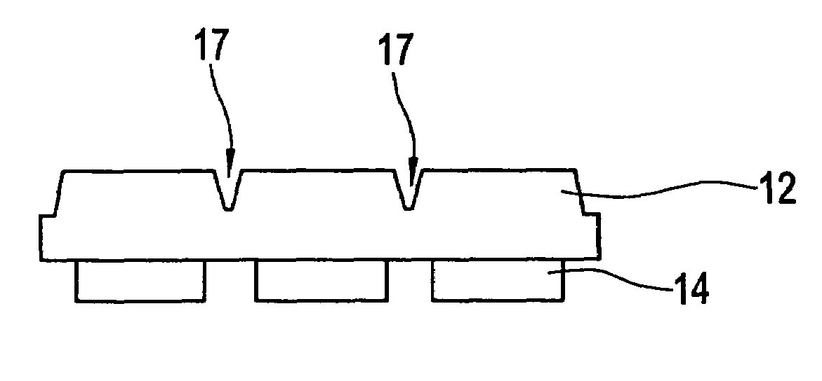
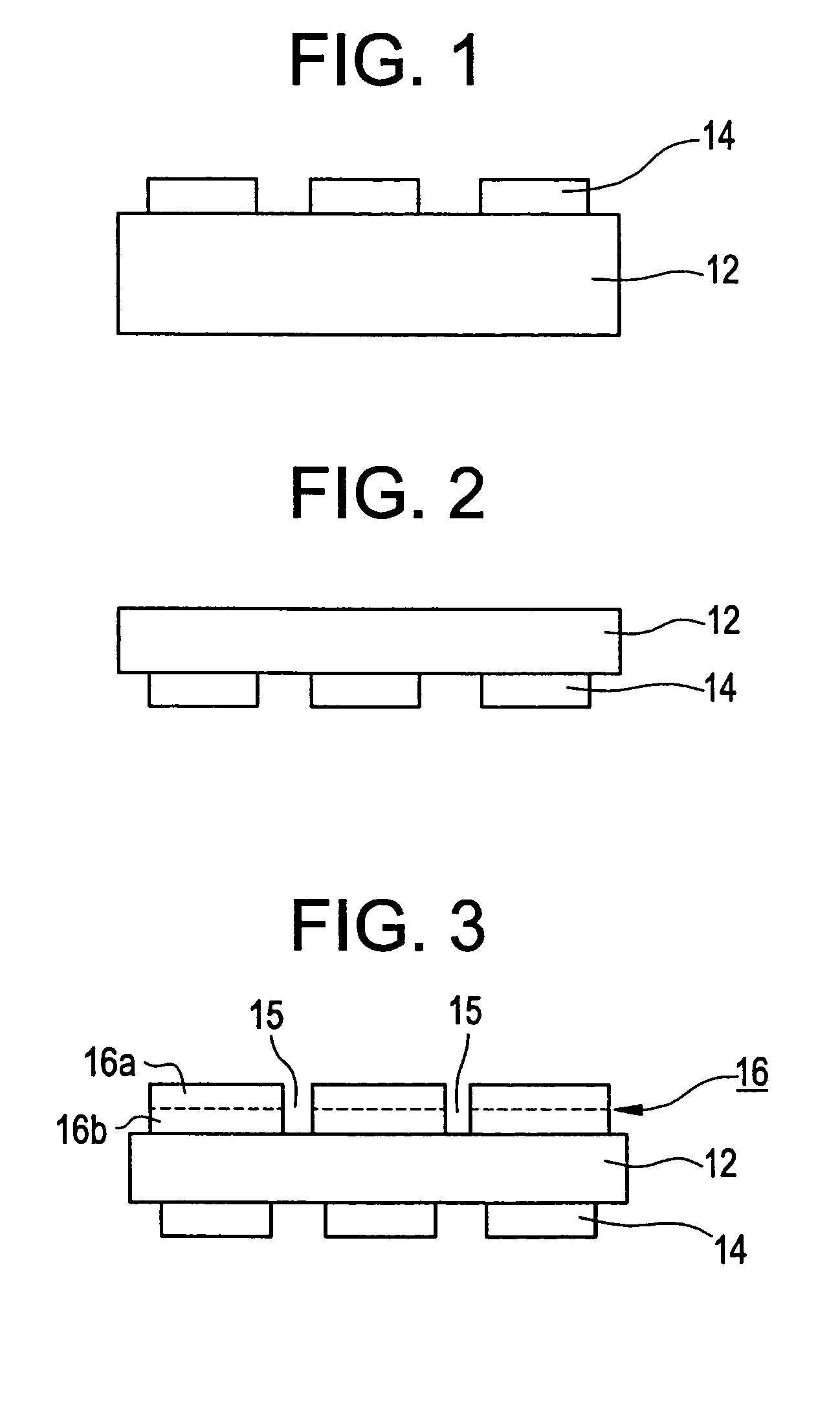
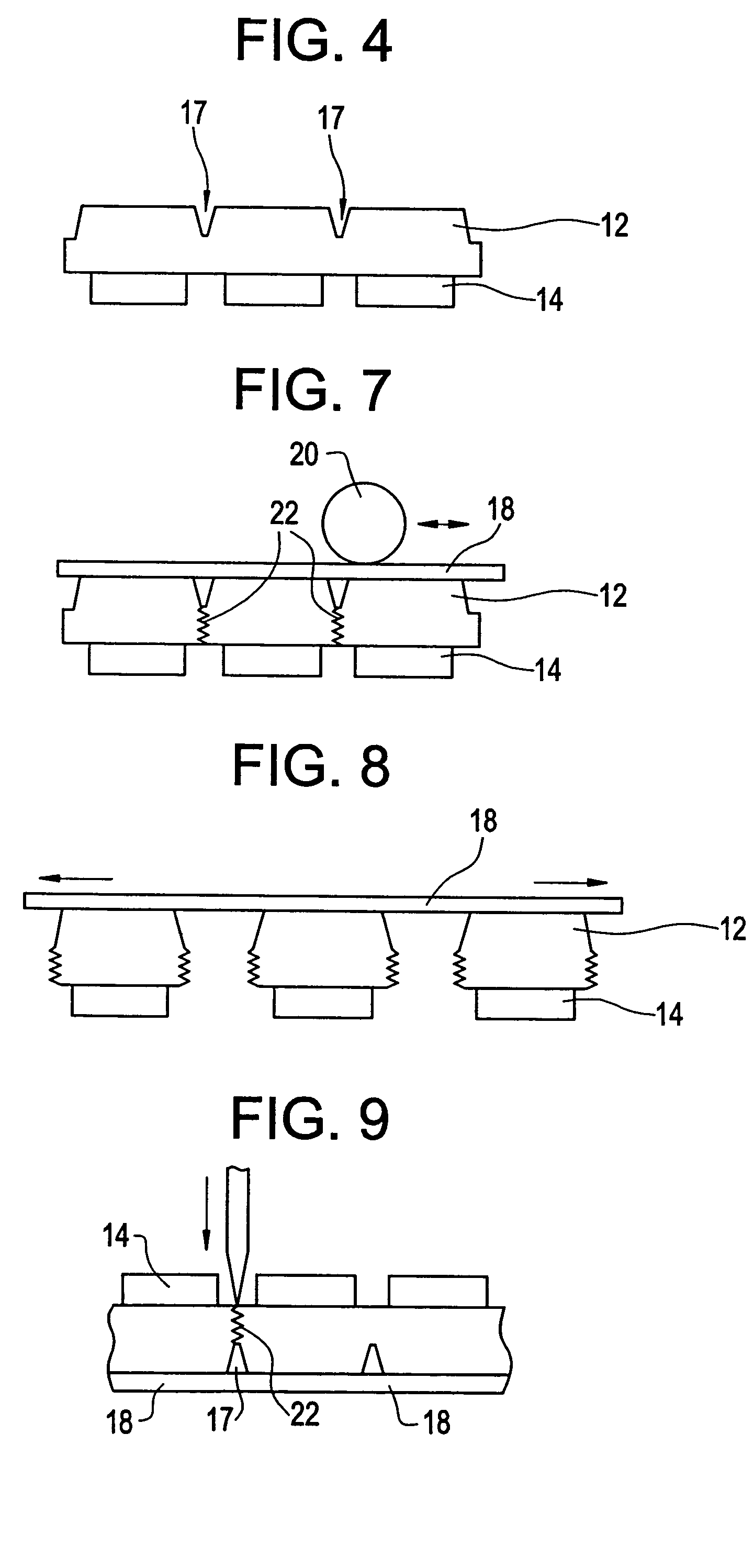
[0033]The following generally describes a process for dicing substrates to separate individual semiconductor devices and a process for thinning substrates. The described processes are particularly advantageous when dicing and thinning hard substrates such as sapphires and SiC. Other substrates that can be used include Si, GaAs, InP, ZnSe, ZnO, and GaP. All semiconductor devices fabricated on a hard semiconductor substrate can be separated with ICP RIE scribing method. Furthermore, some metals can be etched using the described process. However, it should be understood that following describes only some of the many different embodiments that are in accord with the principles of the present invention. Therefore, the present invention is to be understood as encompassing all of the embodiments covered by the claims that follow and by their equivalents.

[0034]The principles of the present invention make use of inductively coupled plasma reactive ion etching (ICP RIE) to separate individual...


PUM

PropertyMeasurementUnit
RF poweraaaaaaaaaa
RF frequencyaaaaaaaaaa
pressureaaaaaaaaaa

Abstract

Thinning and dicing substrates using inductively coupled plasma reactive ion etching (ICP RIE). When dicing, a hard photo-resist pattern or metal mask pattern that defines scribe lines is formed on a sapphire substrate or on a semiconductor epitaxial layer, beneficially by lithographic techniques. Then, the substrate is etched along the scribe lines to form etched channels. An etching gas comprised of BCl3 and / or BCl3 / Cl2 gas is used (optionally, Ar can be added). Stress lines are then produced through the substrate along the etched channels. The substrate is then diced along the stress lines. When thinning, a surface of a substrate is subjected to inductively coupled plasma reactive ion etching (ICP RIE) using BCl3 and / or BCl3 / Cl2 gas, possibly with some Ar. ICP RIE is particularly useful when working sapphire and other hard substrates.

Description

[0001]This application is a continuation of application Ser. No. 10 / 118,318, filed on Apr. 9, 2002, now U.S. Pat. No. 6,818,532.BACKGROUND OF THE INVENTION[0002]1. Field of the Invention[0003]This invention relates to semiconductor fabrication. More specifically, the present invention relates to the use of reactive ion etching in semiconductor fabrication.[0004]2. Discussion of the Related Art[0005]Light emitting diodes, commonly referred to, as “LEDs” are well-known semiconductor devices that convert electrical current into light. The color of the light (wavelength) emitted by an LED depends on the semiconductor material that is used to fabricate the LED. This is because the wavelength of the emitted light depends on the semiconductor material's band-gap energy, which represents the energy difference between valence band and conduction band electrons.[0006]Gallium-Nitride (GaN) has recently gained much attention from LED researchers because GaN has a band-gap energy that is suitabl...

Claims


Application Information

Patent Timeline
Patent Type & Authority Patents(United States)
IPC IPC(8): H01L21/46H01L21/302H01L21/3065G03F9/00H01B13/00H01L21/00H01L21/301H01L21/44H01L21/78H01L33/00
CPCC30B29/20H01L33/0095C30B33/00H01L21/78
Inventor YEOM, GEUN-YOUNGYOO, MYUNG CHEOLURBANEK, WOLFRAMSUNG, YOUN-JOONJEONG, CHANG-HYUNKIM, KYONG-NAMKIM, DONG-WOO
Owner SUZHOU LEKIN SEMICON CO LTD
Why Eureka
Try Eureka