

Apparatus and method for nanoscale pattern generation
a technology of pattern generation and nanoscale, applied in the direction of material nanotechnology, vacuum evaporation coating, coating, etc., can solve the problems of inability to define truly nanoscale features, traditional lithographic methods are approaching theoretical limits, and optical lithographic processes are limited in final resolution
- Summary
- Abstract
- Description
- Claims
- Application Information
AI Technical Summary
Benefits of technology
Problems solved by technology
Method used
Image

Examples
example 1
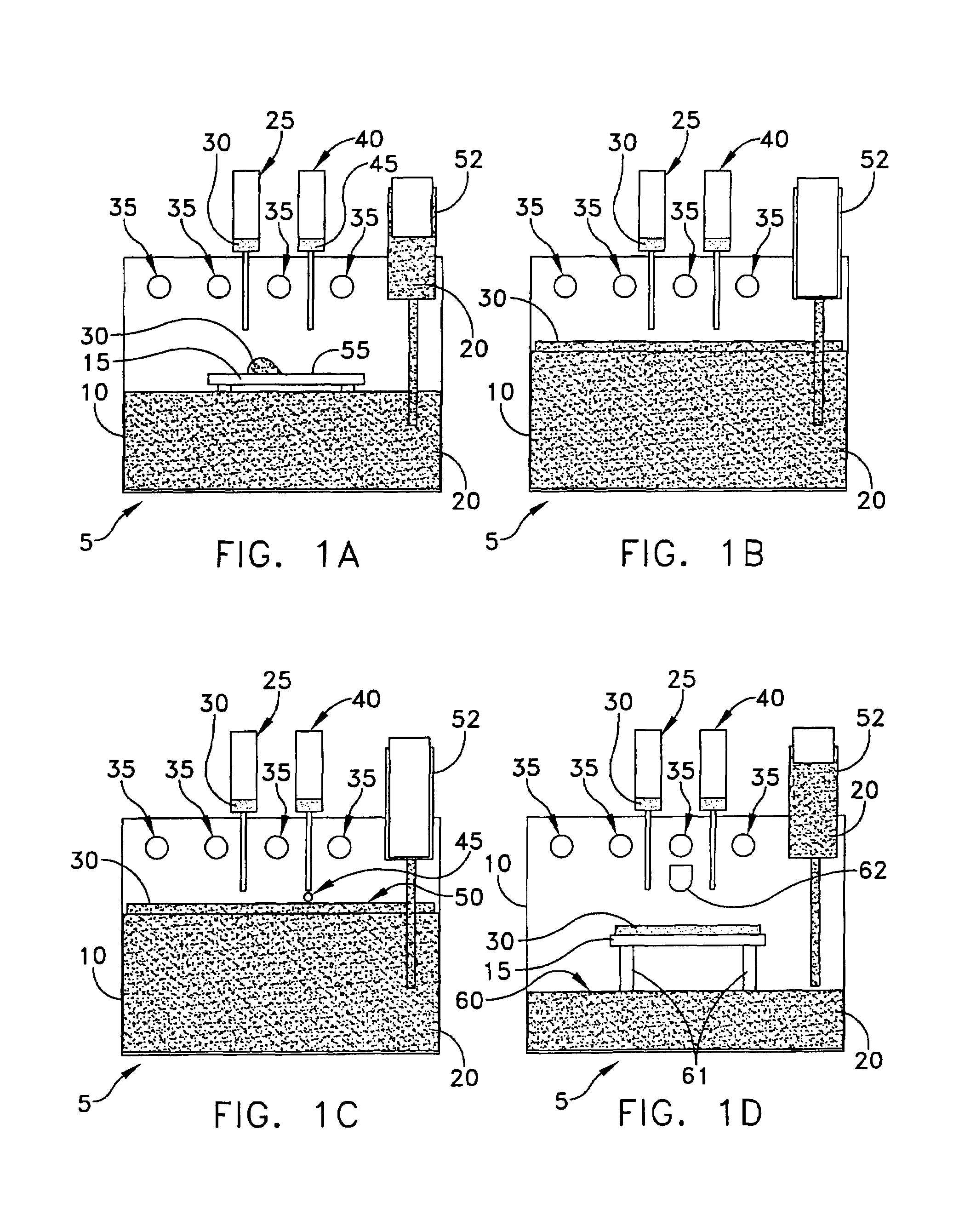
[0051]A silicon substrate was boiled in distilled, deionized water for 20 minutes to produce a hydrophillic surface. Next, the substrate was placed in a heated sample holder to allow thermal control over the substrate. A volume of fluid containing sufficient spheres to cover a 1 cm2 area was drawn into a pipette. The polystyrene spheres in this example were supplied from Interfacial Dynamics Corporation, and were 500 nm in diameter, with sulphatized surfaces. They were shipped in an aqueous solution of 8.2 wt %. The suspension 30 in the pipette was deposited as a droplet on the hydrophilic silicon substrate. The droplet was then covered with a hydrophobic glass cover slide, causing the droplet to spread over a 1 cm2 area of the substrate, thereby forming a monolayer. The glass slide served to limit evaporation of the suspension fluid. Evaporation progressed inwardly from the edge of the droplet, organizing the spheres into a highly ordered monolayer. By limiting the evaporation to o...
example 2
[0052]Monolayers were prepared using monodisperse polystyrene (PS) particles with diameters of 1040, 925, 496, 217 and 127 nm. All particles were purchased from Microparticles GmbH (Germany) as a 10 wt. % suspension. The PS particles have a density of 1.05 g / cm3, a refractive index of 1.59, and a hydrophobic surface. The standard suspension 30 was diluted with an equal amount of ethanol. The suspension 30 was then ultrasonically agitated for 20–30 seconds in a bath to improve mixing. The spheres have a polydispersity index of less than 0.05.
[0053]Oriented (111) p-silicon wafers, boron doped, with resistivity of 1–20 Ωcm and thickness of 525±25 μm, were obtained from SilChem. The surface roughness parameter RA was about 2 nm. These wafers were cut into 10×10 mm or 5×5 mm squares. Each square was thoroughly cleaned with acetone, and additionally in ethanol, in ultrasonic bath for 1 minute. The substrates were dried in a nitrogen atmosphere.
[0054]A solution of PS-latex particles was pr...
example 3
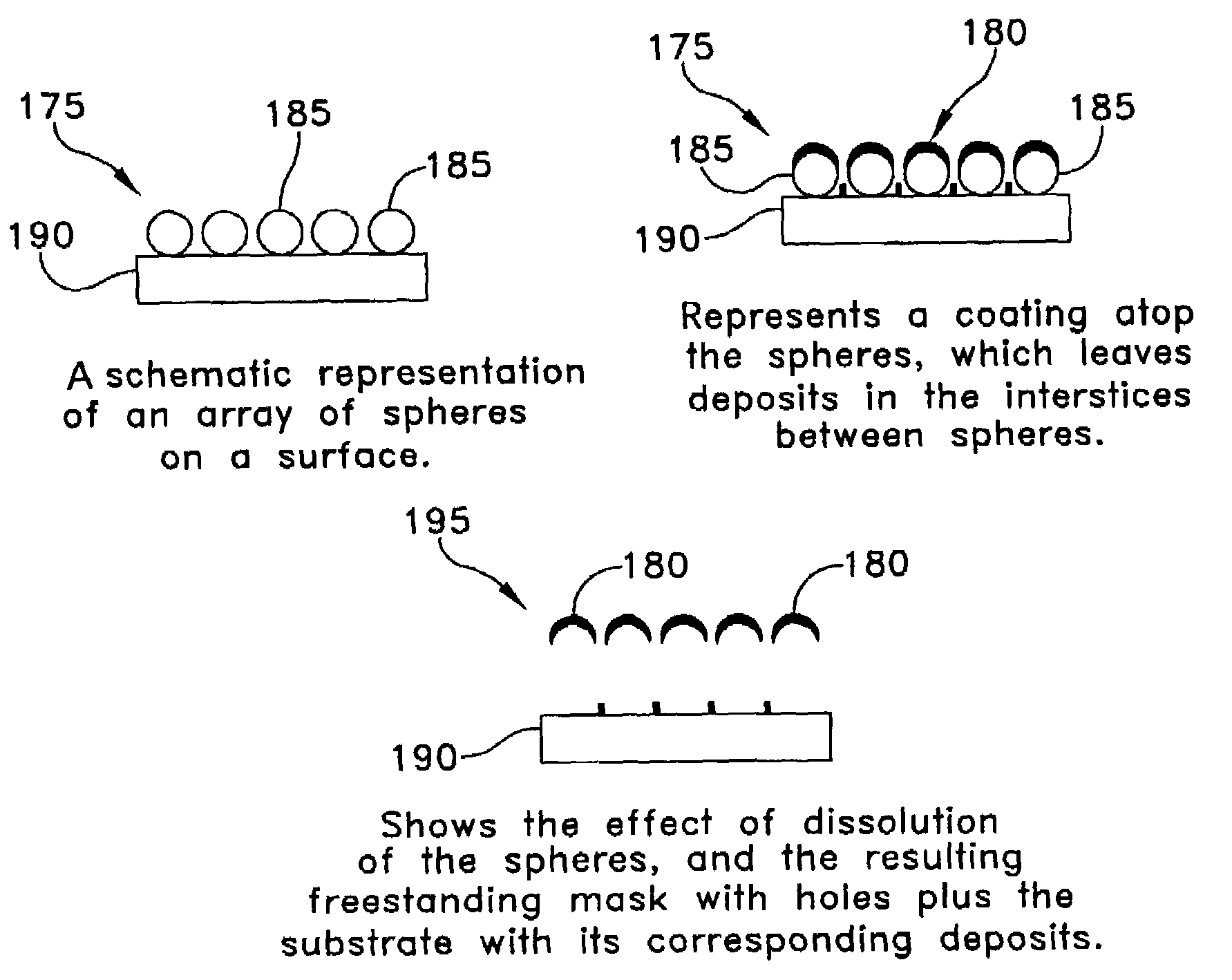
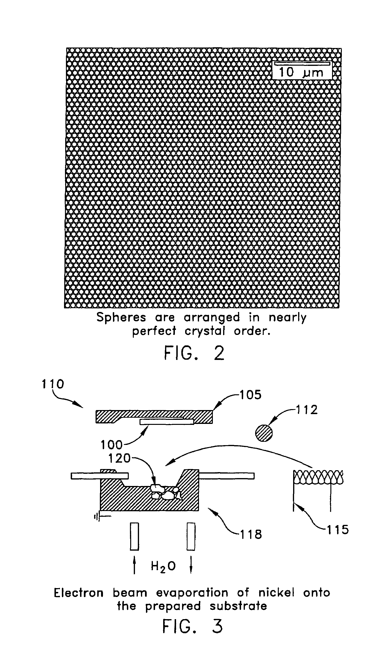
[0055]Looking next at FIG. 3, the samples 100 and 105, produced in Examples 1 and 2 above, were placed in an electron beam evaporator 110, and evacuated to 5×10⁻⁶ mbar. Using a 10 kV acceleration voltage, the electrons 112 produced by a tungsten filament 115 were directed into a crucible 118 holding nickel particles 120. Under these conditions, the nickel 120 is vaporized, and deposits upon surfaces in the chamber, including the samples 100 and 105. The evaporation rate was measured and found to be 1 nm / s under these conditions. With the PS coating, most of the nickel 120 does not reach the substrate surface 100 and 105. However, and looking now at FIG. 4, in the interstices 125 between particles 130, the nickel 120 sees the substrate 105, and is deposited thereon. The deposits form a hexagonal array of triangular shapes 140 between spheres 130. After dissolving spheres 130 in THF (tetrahydrofuran), the remaining pattern 140 on substrate 145 is revealed, as shown in FIG. 5A. After t...
PUM
| Property | Measurement | Unit |
|---|---|---|
| area | aaaaa | aaaaa |
| diameter | aaaaa | aaaaa |
| roughness | aaaaa | aaaaa |
Abstract
Description
Claims
Application Information