Inspection method and apparatus using charged particle beam

a technology of charged particles and beams, applied in the direction of material analysis, semiconductor/solid-state device testing/measurement, instruments, etc., can solve problems such as shading, image distortion and focus deviation or aberration, and uneven charges of wafers, so as to improve inspection accuracy

Inactive Publication Date: 2006-03-28
HITACHI HIGH-TECH CORP
View PDF8 Cites 31 Cited by
  • Summary
  • Abstract
  • Description
  • Claims
  • Application Information

AI Technical Summary

Benefits of technology

[0024]This invention, by controlling the charge of an inspection sample to be more uniform than before, aims to realize an inspection apparatus and method using a charged particle beam that enables acquisition of voltage contrast images of higher quality and provides better inspection and measurement accuracy than conventional ones.
[0029]This invention solves the conventional problem in the inspection process of a partly completed substrate of a semiconductor device that the accuracy of inspection is degraded due to shading on images caused by the charge the substrate had before inspection. Using ultraviolet light instead of an electron beam for charge removal and operating it in coordination with the operation of the charge control electrode enabled control to have a uniform charge over a broad area of the substrate. Further, the improvement of a method of acquiring a image without generating any shading will improve the accuracy of inspection.

Problems solved by technology

As described above, following are the problems with controlling the charge of an inspection sample:(1) Charges can be uneven depending on the circuit patterns in the area for charge control or on the method of charge control,(2) A wafer can be already unevenly charged before it is carried into the charged particle beam apparatus, the polarity of the charge being unknown.
These problems would cause troubles of shading, image distortion and focus deviation or aberration, etc.
These troubles of shading, image distortion and focus deviation, etc. would cause various secondary problems for apparatuses utilizing secondary electron images, for example, degradation of defects inspection accuracy with a SEM type appearance inspection apparatus, degradation of inspection throughput caused by decreased voltage contrast with a review SEM, and degradation of measuring accuracy caused by decreased contrast with a measuring SEM.
Also, with the technology of controlling charges by pre-charging disclosed in JP 2000-208085A, for getting a wafer charged evenly, it is necessary to know the charge distribution on the wafer before performing a pre-charge operation, making it difficult to generate a desired charge.
For example, when a wafer was topically or locally charged, it was difficult to control charging so as for a particular area of the wafer to have a selected charge because the quantity of electric charge and irradiation energy required for the charge control was unknown.

Method used


Image

  • Inspection method and apparatus using charged particle beam
  • Inspection method and apparatus using charged particle beam
  • Inspection method and apparatus using charged particle beam

Examples


embodiment 1

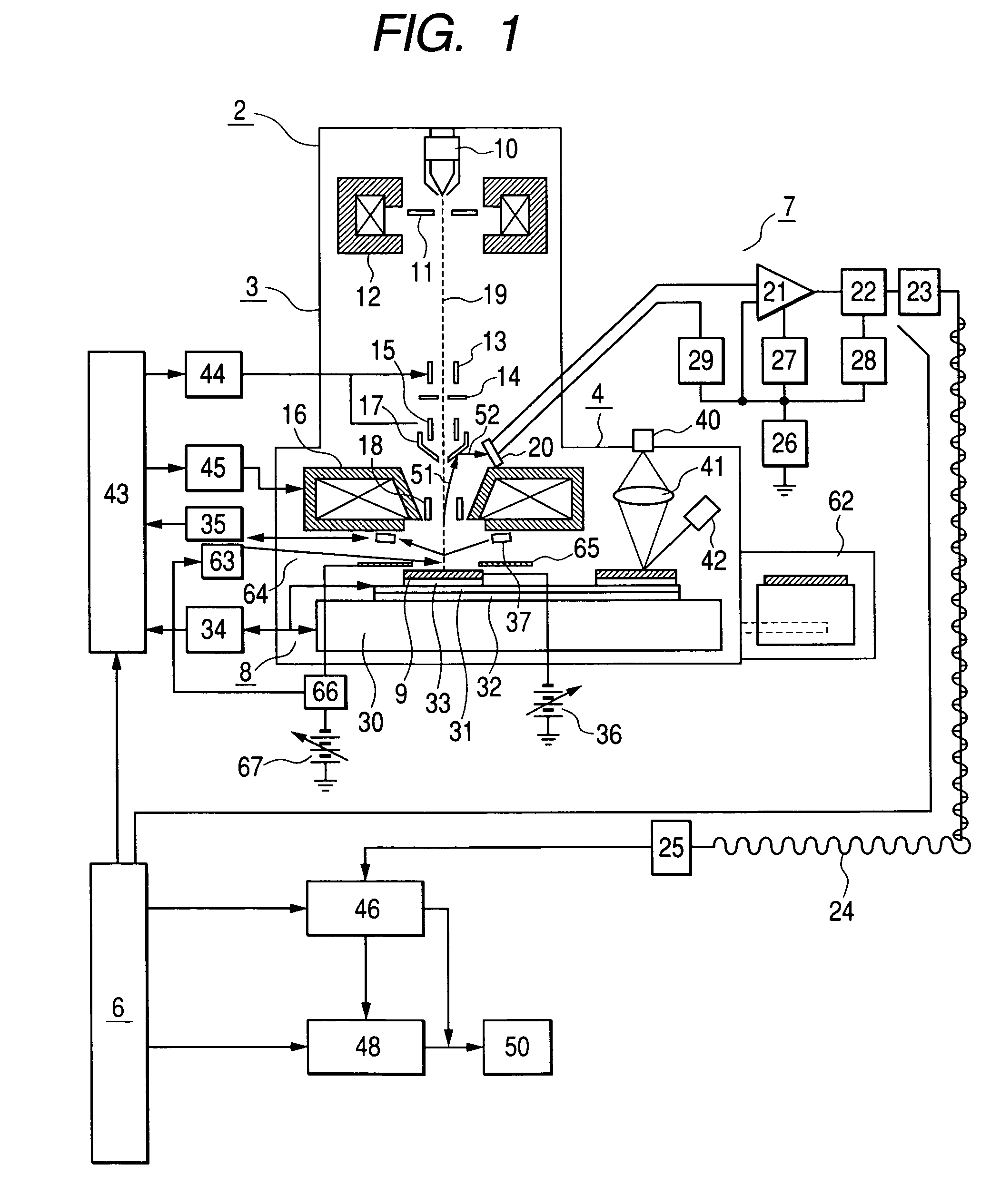
[0058]FIG. 1 shows the configuration of an inspection apparatus relating to the first embodiment of the present invention. The inspection apparatus comprises an inspection chamber 2 inside of which can be evacuated, and a spare chamber (not described in the figure of this embodiment) that is used to transfer a sample substrate 9 into the inspection chamber 2 and configured so as to be evacuated independently of the inspection chamber 2. The inspection apparatus, in addition to the inspection chamber 2 and the spare chamber referred to above, further comprises a control unit 6, and an image processing unit. Inside of the inspection chamber mainly comprises an electro optical system 3, a detection unit, a sample chamber 8, an optical microscope unit 4 and an ultraviolet irradiation system.

[0059]The ultraviolet irradiation system comprises a Ultraviolet light source 63 and a ultraviolet light source control device not shown in the figure, and the ultraviolet light source control device...

embodiment 2

[0089]In accordance with this embodiment of the present invention, a defect inspection is conducted using the inspection apparatus described in the first embodiment, acquiring a voltage contrast image of a wafer that has been charged to a desired voltage.

[0090]In particular, just before the acquisition of an inspection image, a voltage was applied to the charge control electrode to produce a potential barrier to the electrons as high as −5V, and while irradiating ultraviolet, the stage was scanned so as for the wafer to be irradiated with ultraviolet all over the surface. The wafer's charge potential was made almost the same as that of the charge control electrode, and with the ultraviolet irradiation all over the wafer, a uniform charge of −5V across the wafer was attained.

[0091]Then, with the potential of the charge control electrode being set at 1000V elative to the wafer (FIG. 19, step 2210), an inspection is started. The secondary electrons generated by the scan of ultraviolet ...

embodiment 3

[0092]In accordance with this embodiment, an example of performing a length-measurement of a pattern formed on a wafer using a measuring SEM will be explained.

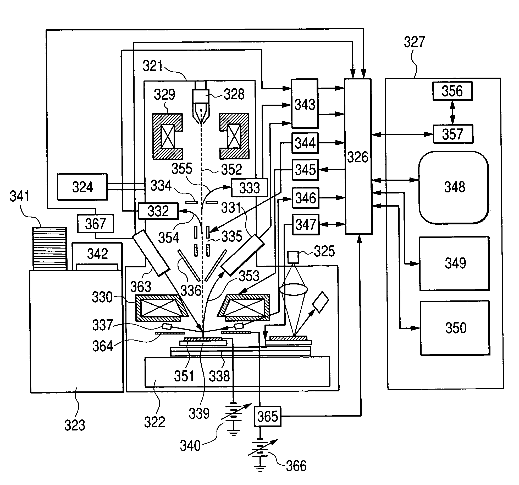
[0093]In FIG. 2 shown is an example of the configuration of a measuring SEM. This apparatus comprises an electro optical system 221, a stage mechanism system 222, a wafer handling system 223, an evacuation system 224, an optical microscope 225, a control system 226 and an operation unit 227. The electro optical system 221 comprises an electron gun 228, a condenser lens 229, an object lens 230, a secondary electron detector 231, an energy filter 234, a deflector 235, a reflector plate 236, and a wafer height detector 237. The stage mechanism system 222 comprises XY stage 238, a holder 239 for loading a sample wafer and a retarding electric source 240 for applying a negative voltage onto the holder 239 and a wafer 251.

[0094]On the XY stage 238, attached is a position detector by laser length measurement. The wafer handling syste...


PUM

PropertyMeasurementUnit
wavelengthaaaaaaaaaa
voltageaaaaaaaaaa
negative voltage contrastaaaaaaaaaa

Abstract

Inspection method and apparatus using a charged particle beam for the inspection of defects on an unfinished semiconductor wafer in the manufacturing process of a semiconductor device, a uniform charge across the wafer is attained by performing ultraviolet irradiation and voltage application to a charge control electrode in a coordinated manner.

Description

CLAIM OF PRIORITY[0001]The present application claims priority from Japanese application JP 2003-405332 filed on Dec. 4, 2003, the content of which is hereby incorporated by reference into this application.BACKGROUND OF THE INVENTION[0002]1. Field of the Invention[0003]This invention generally relates to the method and apparatus for manufacturing substrates having fine circuit patterns, such as semiconductor devices or liquid crystals, especially to the technology for the inspection of patterns for semiconductor devices or photo masks. Further in particular, it relates to the inspection method and apparatus using a charged particle beam for the inspection of defects in any portion on an unfinished semiconductor wafer in the manufacturing process of a semiconductor device.[0004]2. Description of the Related Art[0005]A semiconductor device is produced by repeating the processes of printing a pattern formed on a photo-mask onto a wafer through lithography and etching processes. For the...

Claims


Application Information

Patent Timeline
Patent Type & Authority Patents(United States)
IPC IPC(8): G01N23/00H01J37/20H01J37/22H01J37/28G01R31/302G01R31/311G02F1/1335H01J37/244H01L21/027H01L21/66
CPCG01R31/311
Inventor KOYAMA, HIKARUNISHIYAMA, HIDETOSHINOZOE, MARI
Owner HITACHI HIGH-TECH CORP
Why Eureka
Try Eureka