Very low effective dielectric constant interconnect Structures and methods for fabricating the same

a dielectric constant and interconnect technology, applied in the direction of electrical equipment, semiconductor devices, semiconductor/solid-state device details, etc., can solve the problems of fracture toughness and cohesive strength, low k dielectrics have a much lower elastic modulus, and the mechanical strength of the interconnect structure is also correspondingly inferior, so as to improve the mechanical strength of the interconnect structure

Inactive Publication Date: 2006-04-04
GLOBALFOUNDRIES US INC
View PDF6 Cites 109 Cited by
  • Summary
  • Abstract
  • Description
  • Claims
  • Application Information

AI Technical Summary

Benefits of technology

[0014]A feature of the invention is a method of integration to produce a very low keff structure by minimizing or eliminating the contributions of the hard mask, etch stop and cap layers in the interconnect structure.
[0016]Yet another feature of the invention is a provision of a support dielectric under the interconnect lines to enhance the mechanical strength of the interconnect structure.

Problems solved by technology

With the progress in the transistor device technology leading to the present ultra large scale integration, the overall speed of operation of these advanced chips are beginning to be limited by the signal propagation delay in the interconnection wires between the individual devices on the chips.
Although a tunable range of k values is possible with this set of very low k materials there are several difficulties in integrating these materials with copper interconnects by the dual damascene process described above.
First, these low k dielectrics have a much lower elastic modulus, fracture toughness and cohesive strength than the silicon dioxide or FSG films and their adhesion to typical hard mask layers used in current state of the art copper interconnect is also correspondingly inferior.
This renders the DD process highly impractical from the point of view of manufacturability and yields.
Second, most of the very low k films, in particular the ones that are organosilicate-based, are very sensitive to plasma exposures because of the relative ease of oxidation or cleavage of the Si-organic group linkage (for example, Si-methyl) which results in sites that react with moisture in the ambient to form silanol (Si—OH) groups in the film.
Silanols absorb H2O and hence increase the dielectric constant and the dielectric loss factor of the film significantly thus negating the performance benefits expected from the very low k films.
Since reactive ion etch and plasma etch are key steps required in the formation of the dual damascene trench and via structure as described above and in the removal of photoresists used in patterning the very low k materials, it is very difficult if not impossible to avoid plasma damage of this class of films during a prior art dual damascene integration.
Third, many of the organosilicates tend to react with the highly sensitive photoresist layers used to define the fine interconnect pattern leading to a deterioration of the imaging and resolution capability of the resists.
Additionally, the material make up of the dual damascene interconnect structure significantly degrades the effective dielectric constant (keff).
Although, the effective k can be lowered using the very low k intermetal dielectrics (if they can be successfully integrated), the keff reduction achievable is limited by the presence of higher k dielectric layers typically used for the hard mask and the cap layer described in FIG. 1.
These etch stop layers also have a higher dielectric constant than the very low k dielectrics and hence further degrade the keff of the DD structures containing them.
Further, the thickness of these hard mask, cap and etch stop layers do not scale proportionally with decreasing interconnect layer and IMD thickness expected in future generations.
The result is that the detrimental effect of these high k layers is further aggravated at finer ground rules required for the future microelectronic interconnect structures.
Additionally, this process is not reliably manufacturable due to the fact that the lines are suspended using only the vias as support after the photoresist is stripped which will be extremely fragile to handle and are quite likely to deform when the supporting resist is being removed.
Further, the fill process of the very low k dielectric has to fill under the lines in order to provide support and this is likely to be difficult to achieve.
Even if this does occur the best final structure will only have the mechanically weak very low k dielectric everywhere around and under the lines and this will present delamination problems similar to the standard dual damascene polishing process, when the next level of interconnect is fabricated on top of the filled and planarized structure.

Method used


Image

  • Very low effective dielectric constant interconnect Structures and methods for fabricating the same
  • Very low effective dielectric constant interconnect Structures and methods for fabricating the same
  • Very low effective dielectric constant interconnect Structures and methods for fabricating the same

Examples


Embodiment Construction

[0021]This invention pertains to the very high performance microelectronic chips used in computers, microprocessors, microcontrollers, sensors, communication devices and the like. In particular, the inventive structures described herein pertain to the interconnect wiring networks on such chips, significantly reducing the signal propagation delay associated with these wires. The inventive methods detailed and claimed provide the integration steps required to fabricate these high performance interconnect networks with copper wiring and very low dielectric constant dielectrics.

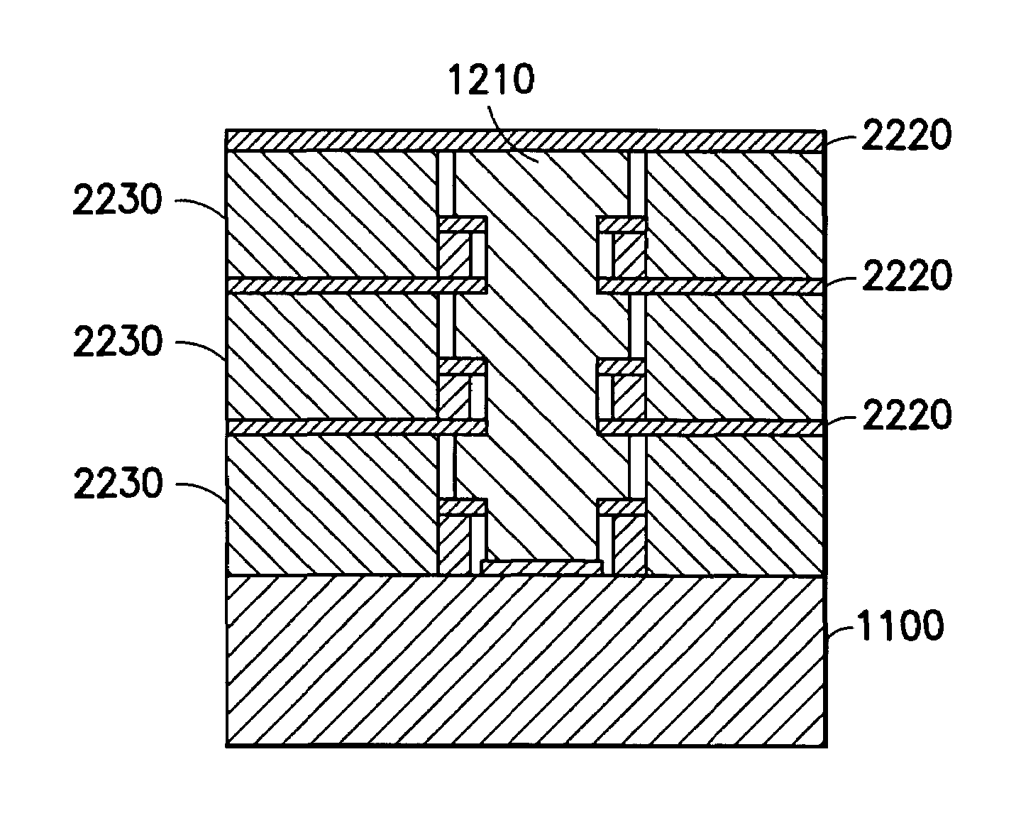
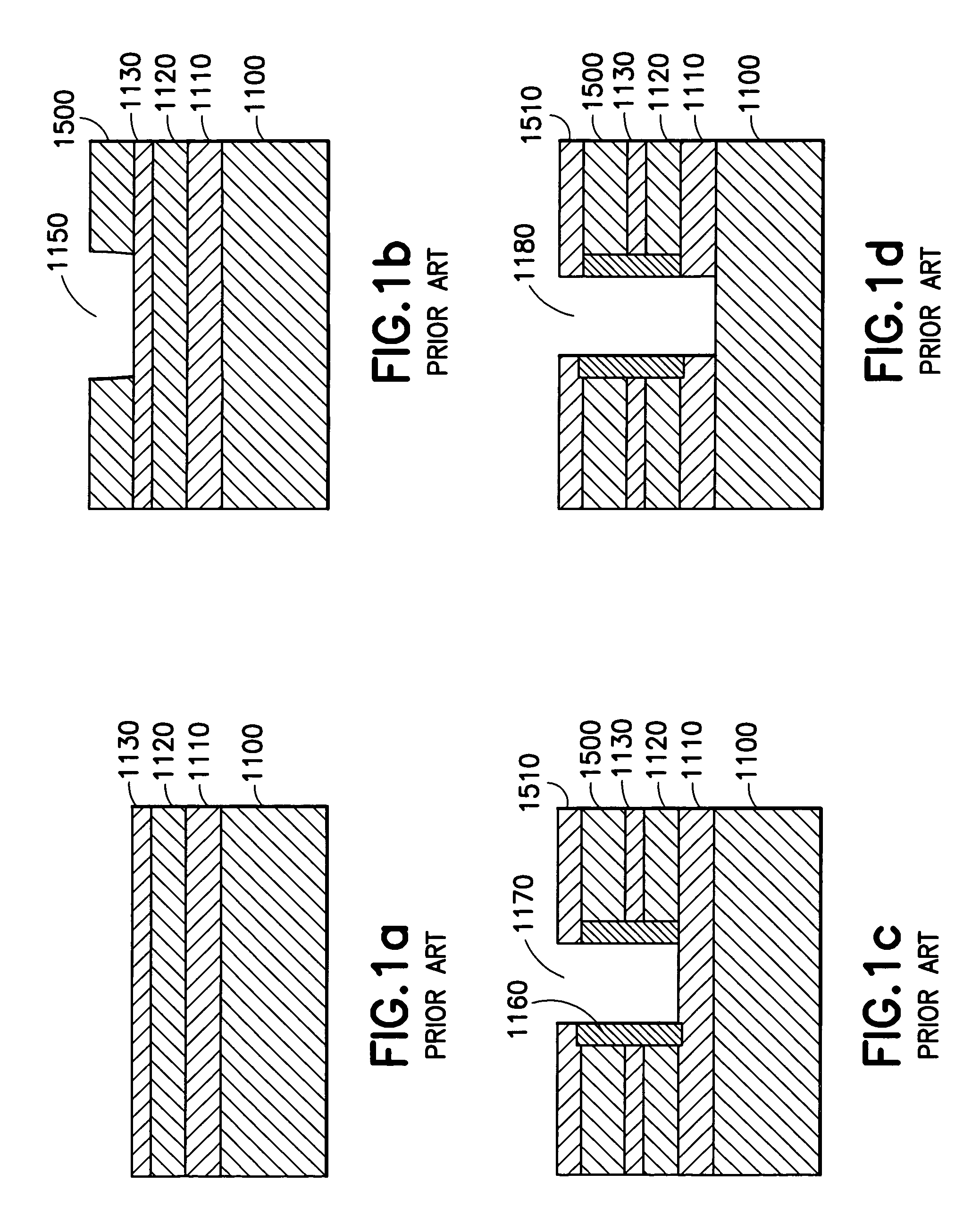
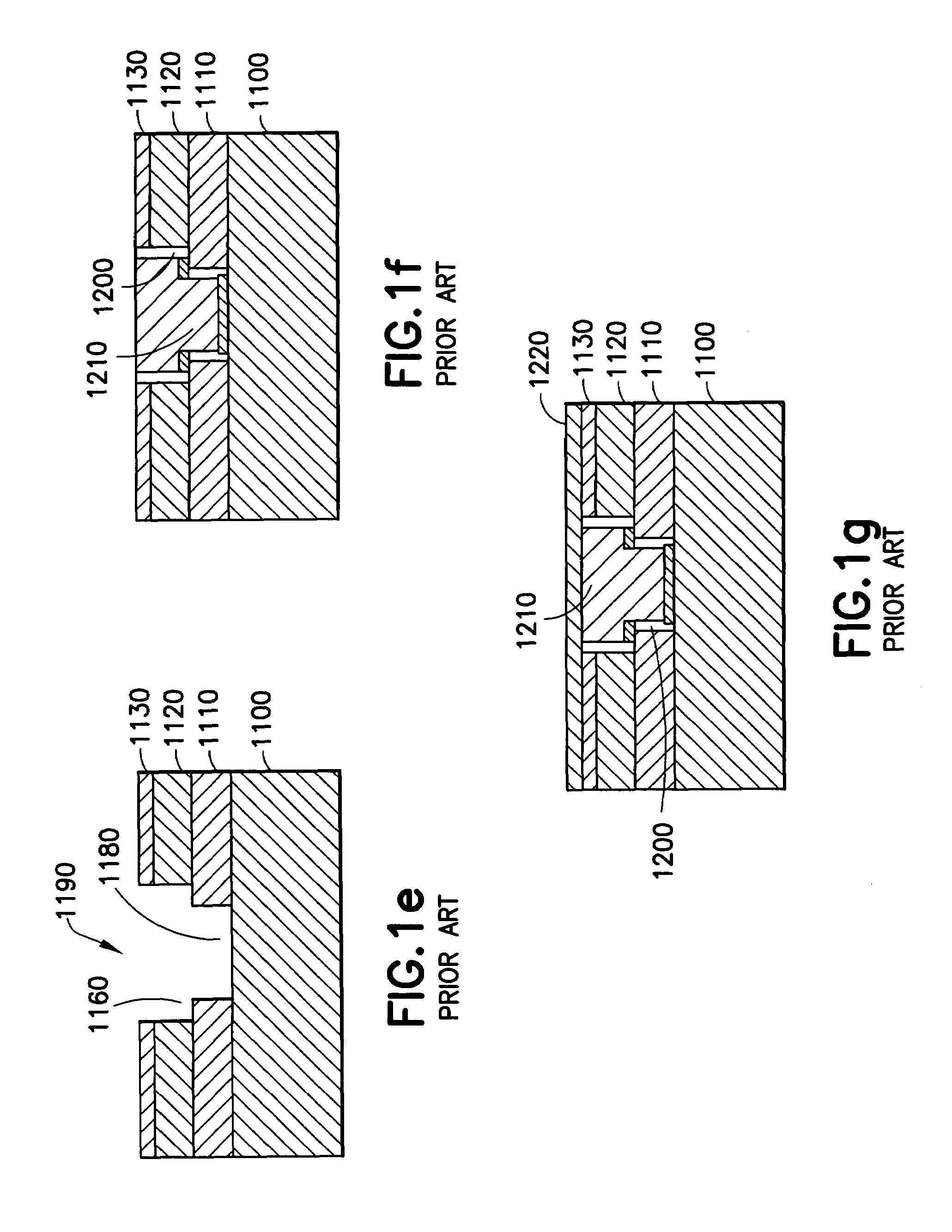
[0022]The inventive method taught is described as the “Etch back and Gap Fill” (EBGF) integration scheme. This method begins with the fabrication of a dual damascene (DD) interconnect structure comprising the prior art steps described earlier and depicted in FIG. 1. The DD structure is built using intermetal dielectric materials (IMD) which are preferably more robust compared to the very low k dielectrics that wi...


PUM

PropertyMeasurementUnit
thicknessaaaaaaaaaa
thickaaaaaaaaaa
thicknessaaaaaaaaaa

Abstract

A structure incorporates very low dielectric constant (k) insulators with copper wiring to achieve high performance interconnects. The wiring is supported by a relatively durable low k dielectric such as SiLk or SiO2 and a very low k and less robust gap fill dielectric is disposed in the remainder of the structure, so that the structure combines a durable layer for strength with a very low k dielectric for interconnect electrical performance.

Description

TECHNICAL FIELD[0001]The field of the invention is “back end of the line (BEOL)” interconnections in high performance integrated circuits and in packaging integrated circuits.BACKGROUND OF THE INVENTION[0002]High performance microprocessor, microcontroller and communication chips require very high speed interconnects between the active transistor devices which are used to perform the various functions such as logical operations, storing and retrieving data, providing control signals and the like. With the progress in the transistor device technology leading to the present ultra large scale integration, the overall speed of operation of these advanced chips are beginning to be limited by the signal propagation delay in the interconnection wires between the individual devices on the chips. The signal propagation delay in the interconnects is dependent on the RC product where R denotes the resistance of the interconnect wires and C represents the overall capacitance of the interconnect...

Claims


Application Information

Patent Timeline
Patent Type & Authority Patents(United States)
IPC IPC(8): H01L23/48H01L21/768
CPCH01L21/76807H01L21/76834H01L21/76835H01L21/76885H01L2924/0002H01L2924/00
Inventor CANAPERI, DONALD F.DALTON, TIMOTHY J.GATES, STEPHEN M.KRISHNAN, MAHADEVAIYERNITTA, SATYA V.PURUSHOTHAMAN, SAMPATHSMITH, SEAN P. E.
Owner GLOBALFOUNDRIES US INC
Why Eureka
Try Eureka