Copper foil for high-density ultrafine printed wiring boad

a copper foil and ultra-fine technology, applied in the field of ultra-fine copper foil, can solve the problems of insulating malfunction, long time required for etching treatment to remove copper nodules, and open circui

Inactive Publication Date: 2006-04-11
FURUKAWA ELECTRIC CO LTD
View PDF10 Cites 38 Cited by
  • Summary
  • Abstract
  • Description
  • Claims
  • Application Information

AI Technical Summary

Benefits of technology

[0032]The present invention relates to an ultra-thin copper foil with a carrier comprising a release layer, a diffusion preventive layer and a copper electroplating layer laminated in this order on the surface of a carrier foil, wherein an outermost surface of the copper electroplating layer is roughened.

Problems solved by technology

However, when a wiring pattern has a narrow line width, it can be resulted in open circuit.
Copper nodules of this roughened surface are pushed into the substrate, and therefore, longer time is required for etching treatment to remove those copper nodules by etching.
If the copper nodules which have been pushed into the substrate were not removed completely, they become residual copper, causing an insulating malfunction when line pitches in a wiring pattern are narrow.
In addition, a relatively thin copper foil having a thickness of 9 μm or 12 μm has a low mechanical strength, thereby easily causing a wrinkle or fold in a production process of a printed wiring board, and sometimes resulting in a breakage of the copper foil.
Therefore, a problem arises such that the most careful attention must be paid in handling thereof.
As is described above, it is practically very difficult to produce a printed wiring board on which a fine wiring pattern is formed, whose Ef value is large, and at the same time, whose contact strength with a substrate is also high.
Particularly, it is virtually impossible to form a wiring pattern of high density and extra-fine wiring with a line pitch and line width of around 30 μm, using a commercially available copper foil.
However, on the other hand, there has been actualized problems as below.
Therefore, when a chromium plating layer is used as a release layer as shown in Japanese Patent Publication No. 16329 / 1978, chromium is dispersed in a copper layer as a carrier causing adhesion of the carrier foil and the ultra-thin copper foil, making release infeasible.
Accordingly, it is impossible to carry out laser drill directly from the surface of the copper foil.
The conformal mask method requires a troublesome process in which an etching resist is coated on a copper electroplating layer 4 in FIG. 1, except for a part on which via holes are aimed to be provided, and after the copper foil is once removed by etching, the resin part is penetrated by combustion with CO2 gas laser.

Method used


Image

  • Copper foil for high-density ultrafine printed wiring boad
  • Copper foil for high-density ultrafine printed wiring boad
  • Copper foil for high-density ultrafine printed wiring boad

Examples


example 1

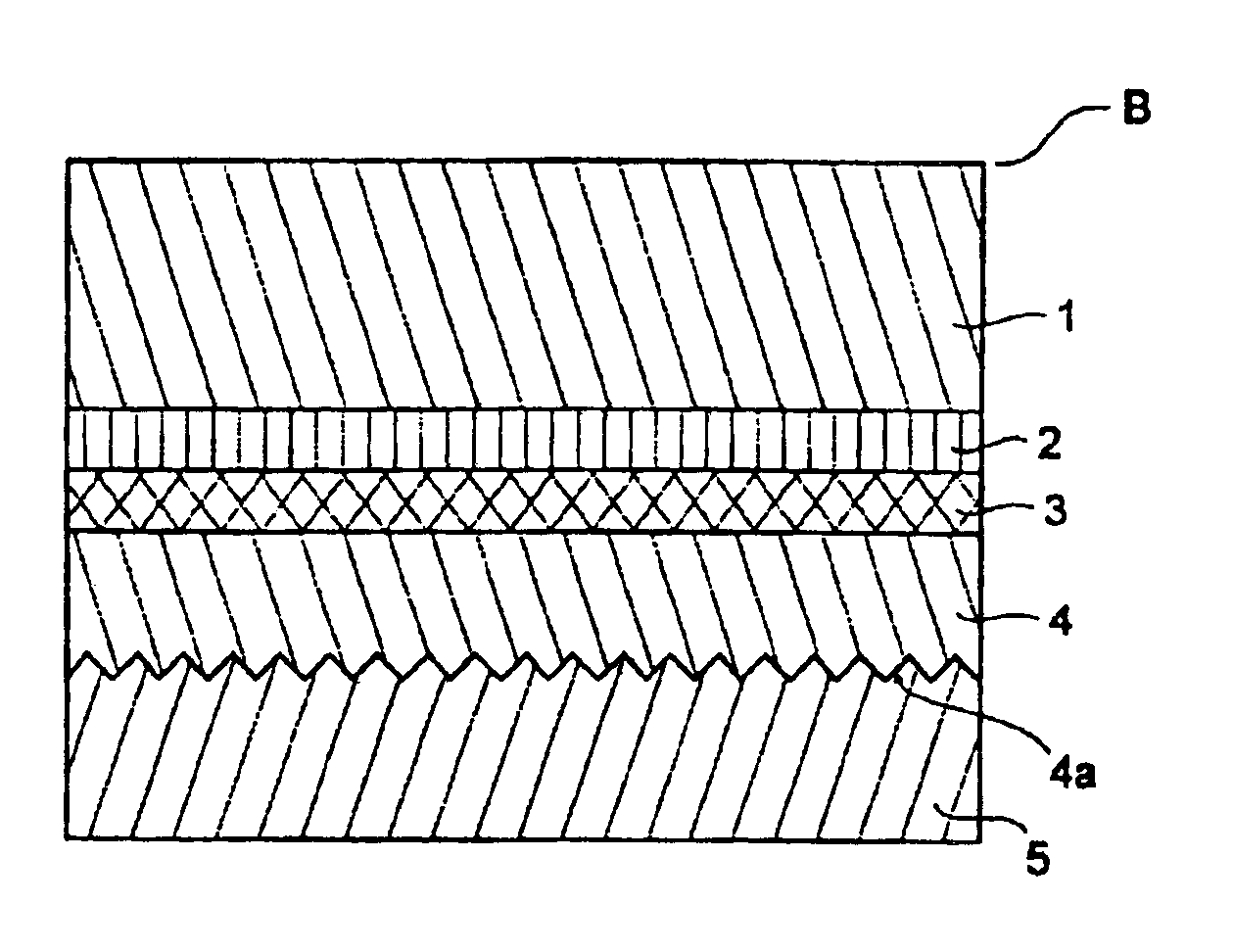
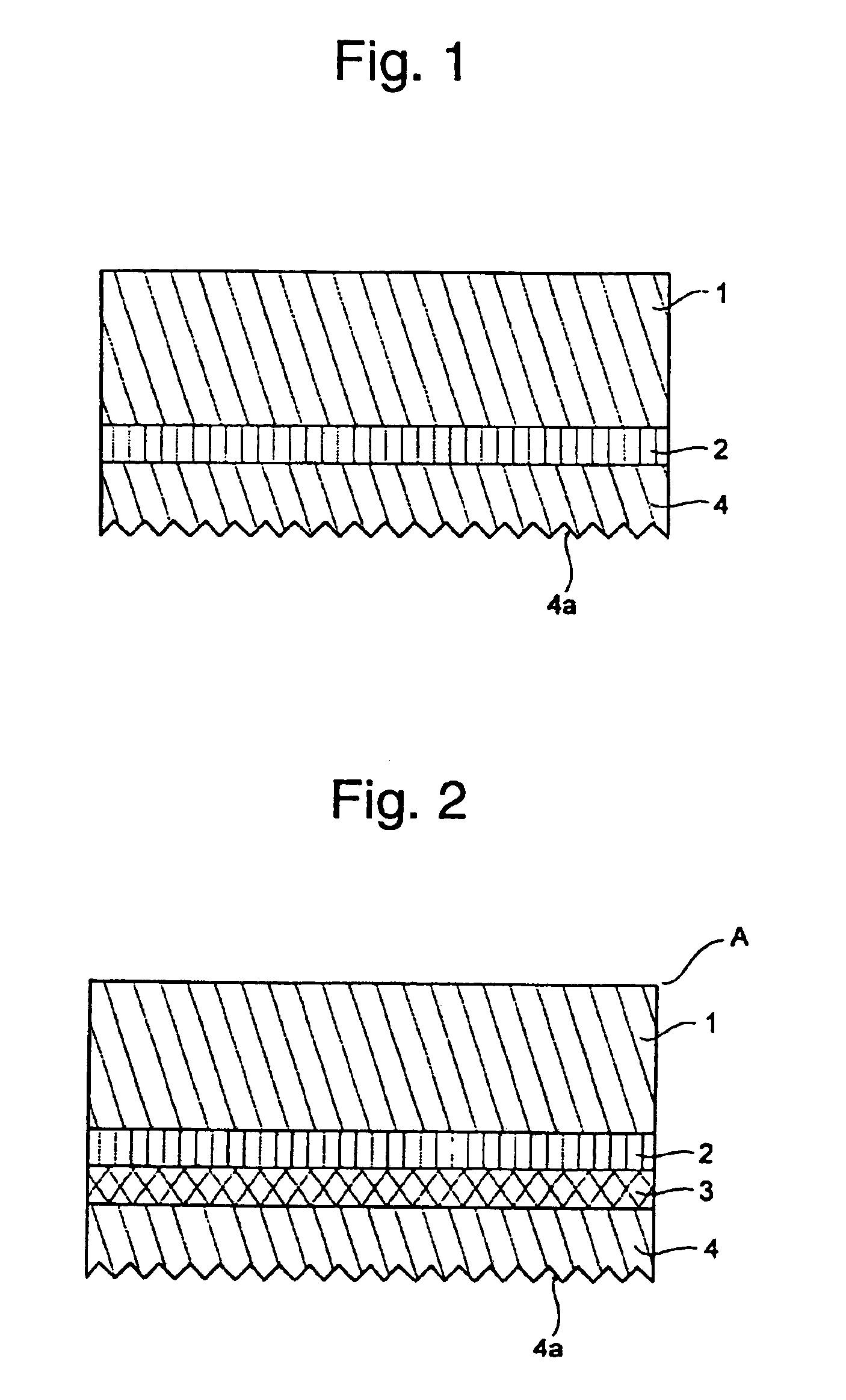
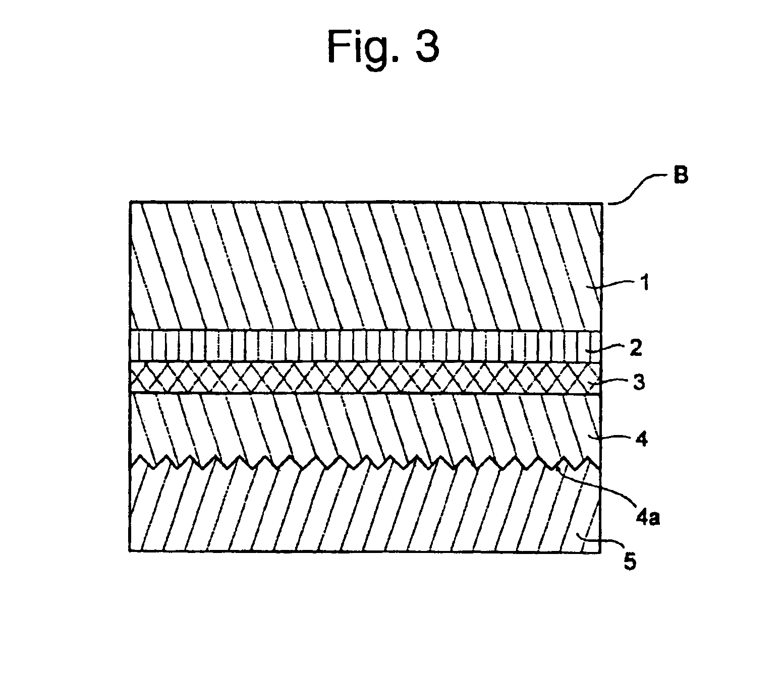
[0091]On a shiny side (shiny side roughness Rz=1.4 μm) of an untreated electrodeposited copper foil with a thickness of 35 μm (a carrier foil 1), an electroplating of chromium was carried out continuously to form a chromium-plating layer (a release layer 2) with an attached amount of 0.50 mg / dm2. Successively, on this chromium-plating layer, Ni—P electroplating was carried out in an aqueous solution having a pH of 4.0 and containing 40.0 g / l of nickel and 1.5 g / l of phosphorus under conditions of current density of 6 A / dm2 to form a diffusion preventive layer. The attached amounts at this moment were 9.1 mg / dm2 for nickel and 0.9 mg / dm2 for phosphorus.

[0092]In addition, on this diffusion preventive layer, electroplating was carried out to form an ultra-thin copper layer with a thickness of 3 μm, using a copper sulfate plating solution containing 80 g / l of copper and 160 g / l of sulfuric acid under current density of 30 A / dm2. And then, surface-roughening treatment was carried out in ...

example 2

[0094]Formation of a release layer 2, formation of a diffusion preventive layer 3, electrochemical deposition of copper, surface-roughening treatment, anticorrosive treatment and surface treatment were carried out in the same manner as in Example 1, except that a diffusion preventive layer was formed by Ni—Co electroplating in an aqueous solution having a pH of 3.5 and containing 40.0 g / l of nickel and 7.5 g / l of cobalt under conditions of current density of 6 A / dm2. Attached amounts by plating of the diffusion preventive layer 3 were 3.9 mg / dm2 for nickel and 6.1 mg / dm2 for cobalt.

example 3

[0095]Formation of a release layer 2, formation of a diffusion preventive layer 3, electrochemical deposition of copper, surface-roughening treatment, anticorrosive treatment and surface treatment were carried out in the same manner as in Example 1, except that a diffusion preventive layer was formed by electrolytic Co—Cu plating in an aqueous solution having a pH of 3.5 and containing 8.0 g / l of cobalt and 4.0 g / l of copper under conditions of current density of 2.0 A / dm2. Attached amounts by plating of the diffusion preventive layer were 8.8 mg / dm2 for cobalt and 1.2 mg / dm2 for copper.


PUM

PropertyMeasurementUnit
particle sizeaaaaaaaaaa
thicknessaaaaaaaaaa
thicknessaaaaaaaaaa

Abstract

The present invention is to provide an ultra-thin copper foil with a carrier which comprises a release layer, a diffusion preventive layer and a copper electroplating layer laminated in this order, or a diffusion preventive layer, a release layer and a copper electroplating layer laminated in this order on the surface of a carrier foil, wherein a surface of the copper electroplating layer is roughened; a copper-clad laminated board comprising the ultra-thin copper foil with a carrier being laminated on a resin substrate; a printed wiring board comprising the copper-clad laminated board on the ultra-thin copper foil of which is formed a wiring pattern; and a multi-layered printed wiring board which comprising a plural number of the above printed wiring board being laminated.

Description

[0001]This application is the United States national phase application of International Application PCT / JP01 / 08220 (not published in English) filed Sep. 21, 2001.TECHNICAL FIELD[0002]The present invention relates to an ultra-thin copper foil with a carrier which is used in producing a printed wiring board to be used for fine pattern, especially to an ultra-thin copper foil with a carrier that enables a production of a copper clad laminated board from a resin substrate which requires casting or pressing at a high temperature, and enables a process of drilling holes by CO2 laser directly through the copper foil.BACKGROUND ART[0003]A printed wiring board has been produced as following.[0004]First, a thin copper foil for surface circuit formation is placed on a surface of an electric insulating substrate comprising a glass-epoxy resin or a glass-polyimide resin, etc., and then, it is heated under pressure to prepare a copper clad laminated board.[0005]Subsequently, on this copper clad l...

Claims


Application Information

Patent Timeline
Patent Type & Authority Patents(United States)
IPC IPC(8): B32B15/08B32B9/00B32B15/20C25D1/04C25D5/10C25D7/06H05K3/02
CPCB32B15/08C25D1/04C25D5/10C25D7/0614H05K3/025B32B15/20Y10T428/12535Y10T428/12514Y10T428/12611Y10T428/12771Y10T428/12493Y10T428/12431Y10T428/24917Y10T428/12569Y10T428/12861Y10T428/31678Y10T428/31681H05K3/38
Inventor SUZUKI, AKITOSHIFUKUDA, SHINHOSHINO, KAZUHIRONAKAOKA, TADAO
Owner FURUKAWA ELECTRIC CO LTD
Why Eureka
Try Eureka