High linearity smart HBT power amplifiers for CDMA/WCDMA application

a power amplifier and high linearity technology, applied in the field of linear power amplifiers, can solve the problems of diode draw current, significant diode draw current, and inefficient traditional bias circuit topologies for precise control of quiescent bias and dynamic operating point, so as to improve the rf efficiency and stability of the combiner, and the effect of high transistor gain

Active Publication Date: 2006-04-11
CALLAHAN CELLULAR L L C
View PDF9 Cites 52 Cited by
  • Summary
  • Abstract
  • Description
  • Claims
  • Application Information

AI Technical Summary

Benefits of technology

[0011]In one aspect of the invention, a power device may have larger sized transistor unit cells, because the inventors have discovered that larger size transistors have higher power gain at lower frequency. A power device may include an 84 square micrometer horseshoe unit cell HBT. In another aspect of the invention, a unit cell transistor may include a horseshoe-shaped emitter and a strip-shaped base geometry to provide higher transistor gain.
[0012]In another aspect, the output power transistor may use a two level 4 way transistor combining technique to combine 4 pairs of transistor arrays (or larger transistor cells) with bonding wires to the output micro strip transmission lines constructed on the laminated substrate. Collectors of two transistor arrays are con

Problems solved by technology

A typical operating temperature range for a mobile phone is −30° to +85° C., which presents additional challenges for the power amplifier.
Traditional bias circuit topologies are inefficient in the precise control of the quiescent bias and dynamic operating point especially at temperature extremes.
The diode bias technique has good temperature compensation, but the diode draws current, which may be significant.
The simple current mirrors do not track as well over temperature.
In addition to improved PA efficiency and bias circuitry, a third issue is to maintain an acceptable system-required amplifier gain with minimum number of power amplifier stages, because the PA also amplifies receive band noise power at the receive frequencies.
The noise power interferes with a downlink signal in the handset's receiver and reduces the dynamic range of the rece

Method used


Image

  • High linearity smart HBT power amplifiers for CDMA/WCDMA application
  • High linearity smart HBT power amplifiers for CDMA/WCDMA application
  • High linearity smart HBT power amplifiers for CDMA/WCDMA application

Examples


Embodiment Construction

[0022]The HBT cell unit size is described.

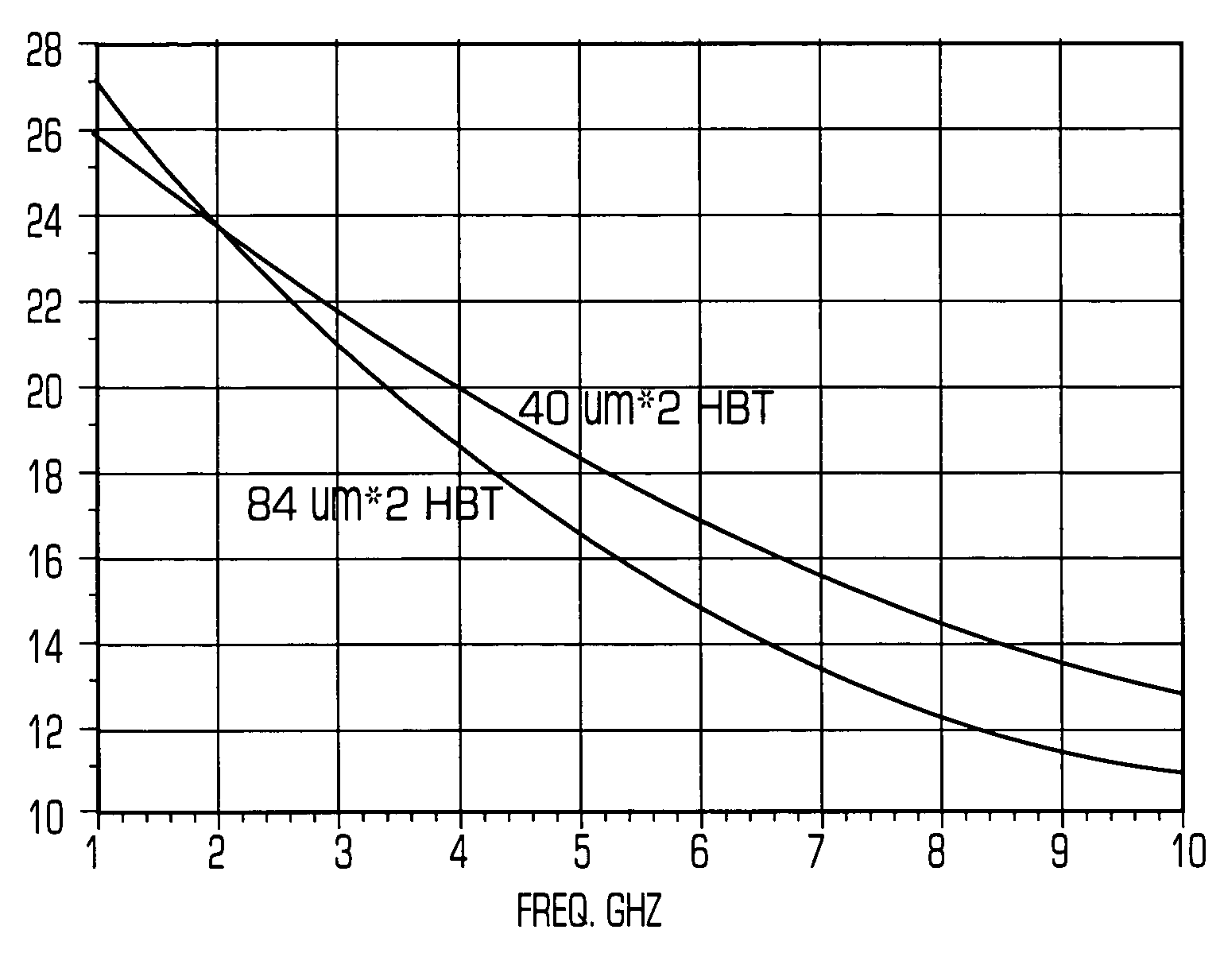
[0023]The emitter ballast resistors are believed to help the thermal stability of power HBT. However, a portion of the output power is dissipated in those resistors and this reduces PAE, particularly at a low supply voltage. Extensive reliability tests revealed that power HBT's can be operated with no emitter ballast resistors without the thermal runaway phenomenon with a lower emitter current density. The present invention relates to an improved design comprising a robust HBT and circuit topologies that includes optimum unit HBT geometry with proper base resistance for RF stability, and efficient unit device combining topology with combining odd mode resistors and a novel active device bias with switch sensing smart function capability. To further improve PAE an optimum HBT geometry and an optimum HBT combining art are selected. The inventors have discovered that larger size transistors have higher power gain at lower frequency.

[0024]FIG. 1...


PUM


Abstract

A power amplifier includes larger size transistors to provide higher power gain at lower frequencies. Transistors of transistor unit cells include a horseshoe-shaped emitter and a strip-shaped base to increase gain. Transistors are combined at a first level to form transistor arrays, which are combined with bonding wires at a second level to an output micro strip transmission line. A Vbe referenced bias circuit may include a smart function to lower quiescent current.

Description

CROSS-REFERENCE TO RELATED APPLICATIONS[0001]This application claims the benefit of U.S. Provisional Application No. 60 / 449,201, filed Feb. 21, 2003, which is incorporated herein by reference.BACKGROUND[0002]The invention relates to power amplifiers, and more particularly to linear power amplifiers.[0003]Current and future digital mobile hand-held communication systems, particularly with code-division multiple access (CDMA), use high efficiency, high linearity, and low cost power amplifiers (PA) for hand held transmitters. Gallium arsenide (GaAs) based heterojunction bipolar transistors (HBT's) are a proven candidate due to their superior power characteristics even at low bias voltages with only a single power supply. In addition to high efficiency and good linearity, the power amplifiers should work at temperature extremes. A typical operating temperature range for a mobile phone is −30° to +85° C., which presents additional challenges for the power amplifier. Traditional bias circ...

Claims


Application Information

Patent Timeline
IPC IPC(8): H03F3/68
CPCH03F1/0261H03F3/189H03F3/211H03F3/602H03F3/60H03F2200/75H03F2200/18H03F2200/366
Inventor ESFANDIARI, REZACHO, NAM-MINCANILAO, ALZON B.GREEN, RONYOO, HYUNGMO
Owner CALLAHAN CELLULAR L L C
Why Eureka
Try Eureka