Light emitting device, semiconductor device, and method of fabricating the devices

a technology of semiconductor devices and light-emitting devices, which is applied in the direction of identification means, instruments, optics, etc., can solve the problems of easy cracking and heavy, glass substrates and quartz substrates are difficult to be made larger, and cannot help lowering the highest temperature of the process, so as to achieve limited deterioration due to water and oxygen permeation

Inactive Publication Date: 2006-05-16
SEMICON ENERGY LAB CO LTD
View PDF68 Cites 222 Cited by
  • Summary
  • Abstract
  • Description
  • Claims
  • Application Information

AI Technical Summary

Benefits of technology

[0013]According to the present invention, a layer to be debonded, containing elements, is formed on a substrate, bonded to a supporting member, and debonded from the substrate, a thin film is thereafter formed in contact with the debonded layer, and the debonded layer with the thin film is adhered to a transfer member. The thin film is grown in contact with the debonded layer to repair cracks caused in the debonded layer at the time of debonding. As the thin film in contact with the debonded layer, a film having thermal conductivity, e.g., film of aluminum nitride or aluminum nitroxide is used. This film dissipates heat from the elements and therefore has the effect of limiting degradation of the elements as well as the effect of preventing deformation and change in quality of the transfer member 22, e.g., a plastic substrate. The film having thermal conductivity also has the effect of preventing mixing of impurities such as water and oxygen from the outside.
[0037]In the above-described arrangement relating to the method of fabricating a semiconductor device, if a light emitting device using an element typified by an OLED is fabricated, it is desirable that the light emitting element be completely isolated from the outside with the supported member used as a sealing member to prevent materials such as water and oxygen which accelerate degradation of an organic compound layer from entering from the outside. Specifically, in such a case, it is characterized in that the element is a light emitting element.
[0039]To facilitate debonding, a granular oxide material may be provided on the nitride layer and an oxide layer for covering the granular oxide material may be provided , thus making separation easier.

Problems solved by technology

At present, although many glass substrates and quartz substrates are utilized, there are defaults of being easily cracked and heavy.
Moreover, the glass substrates and quartz substrates are difficult to be made larger in therms of conducting a mass-production, and these are not suitable for that.
However, since the heat resistance of a plastic film is low, it cannot help lowering the highest temperature of the process.
As a result, at present, a TFT is formed which has not so excellent electric characteristics compared with those formed on the glass substrates.
Therefore, a liquid crystal display device and light emitting element having a high performance by utilizing a plastic film have not been realized yet.
Therefore, light emitting devices using plastic substrates tend to have a shorter life.
Also, generally speaking, substrates formed of plastic film or the like are not resistant to heat.
If the temperature at which an insulating film of silicon nitride or silicon nitroxide is formed on a plastic substrate is excessively high, the substrate deforms easily.
If the film forming temperature is excessively low, a reduction in film quality results and it is difficult to effectively limit permeation of water and oxygen.
There is also a problem in that when a device formed on a plastic film substrate or the like is driven, heat is locally produced to deform a portion of the substrate or to change the quality thereof.
Further, if the thickness of the insulating film of silicon nitride or silicon nitroxide is increased in order to prevent permeation of water and oxygen, a larger stress is caused in the film and the film cracks easily.
If the film thickness is large, the film cracks easily when the substrate is bent.
Also, a layer to be debonded may crack when it is bent at the time of separation from the substrate.

Method used


Image

  • Light emitting device, semiconductor device, and method of fabricating the devices
  • Light emitting device, semiconductor device, and method of fabricating the devices
  • Light emitting device, semiconductor device, and method of fabricating the devices

Examples


embodiment 1

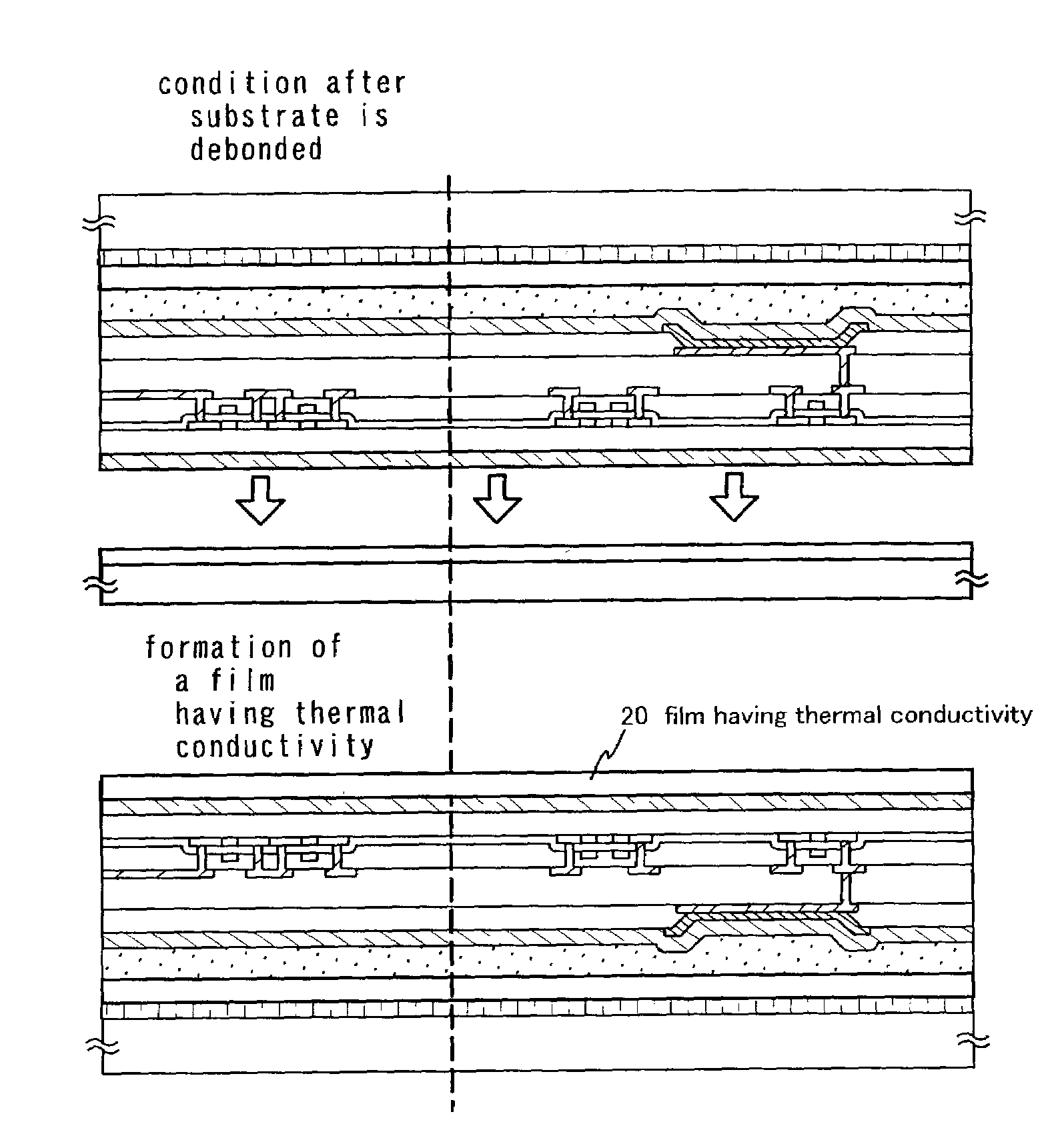
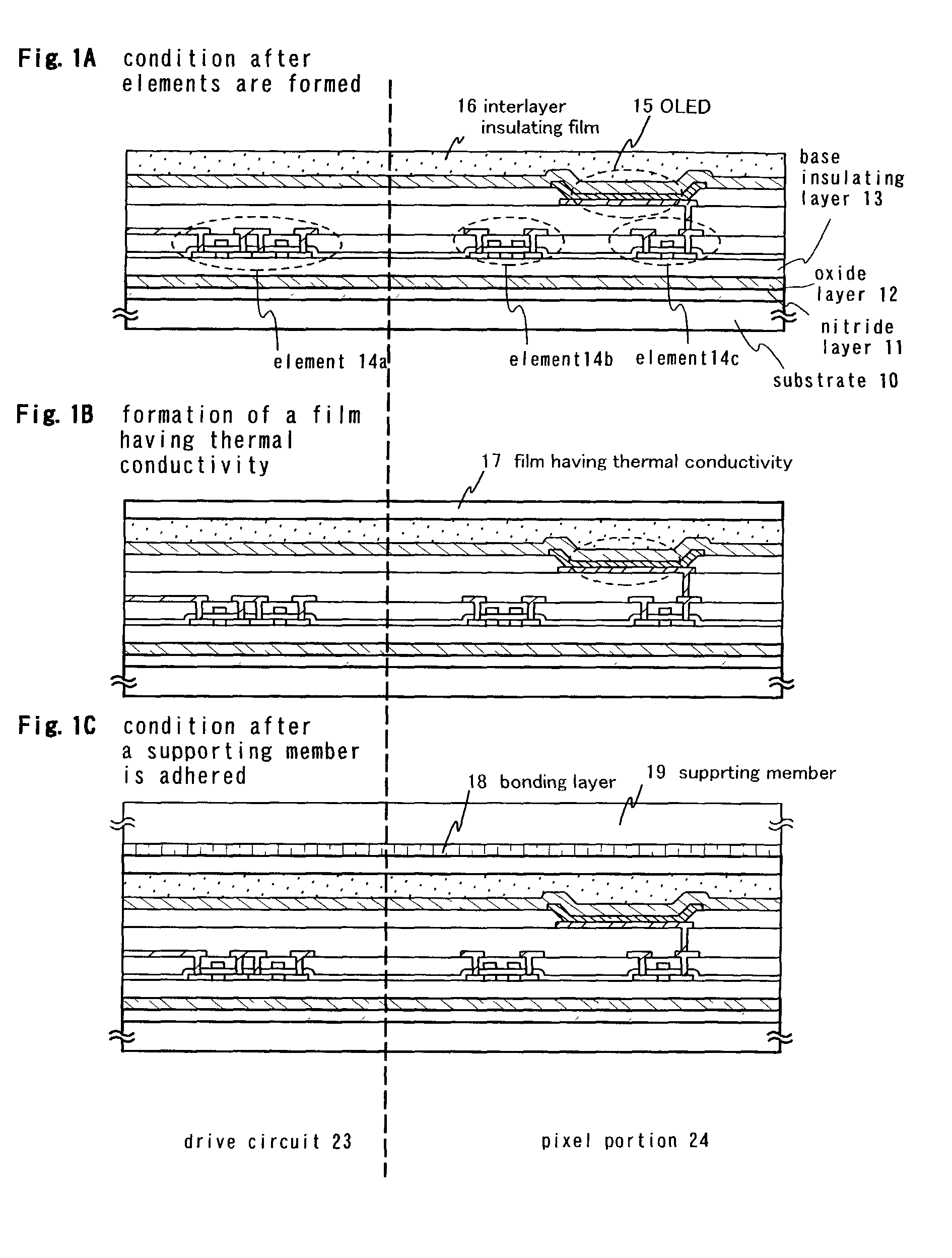
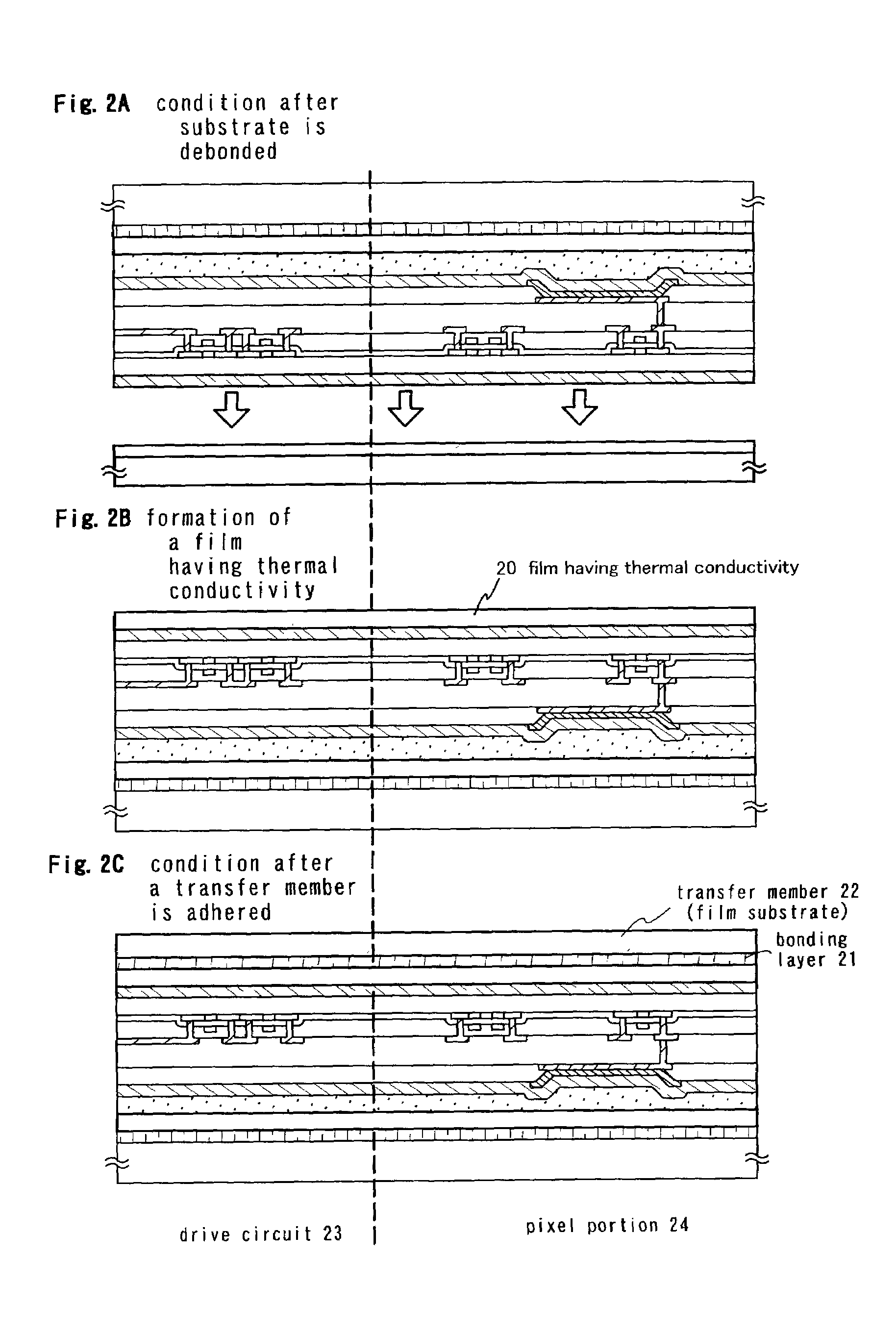
[0132]An example of fabrication of a light emitting device having an OLED and using the TFTs obtained in accordance with Embodiment 1 will be described with reference to FIG. 5.

[0133]FIG. 5 shows an example of a light emitting device (in a state before sealing) having a pixel portion and a drive circuit for driving the pixel portion, the pixel portion and the drive circuit being formed on one insulating member. A CMOS circuit forming a basic unit in the drive circuit and one pixel in the pixel portion are illustrated. The CMOS circuit can be obtained in accordance with Embodiment 1.

[0134]Referring to FIG. 5, a substrate 200, a nitride layer 201 and an oxide layer 202 are provided. On a base insulating layer 203 formed on the element formation substrate, the drive circuit 204 constituted of an n-channel TFT and a p-channel TFT, a switching TFT, which is a p-channel TFT, and a current control TFT, which is an n-channel TFT, are formed. In this embodiment, each of the TFTs is formed as...

embodiment 2

[0165]While an example of use of the top gate TFT in Embodiment 2 has been described, a bottom gate TFT can also be used. An example of an arrangement using a bottom gate TFT will be described with reference to FIG. 8.

[0166]As shown in FIG. 8, each of an n-channel TFT 913, a p-channel TFT 914, and an n-channel TFT 911 is of the bottom gate structure. The TFTs in the bottom gate structure may be fabricated by using well-known techniques. The active layer of these TFTs may be a semiconductor film having a crystalline structure (e.g., polysilicon) or a semiconductor film having an amorphous structure (e.g., amorphous silicon).

[0167]In FIG. 8 are illustrated a flexible film substrate 900 (e.g., a plastic substrate), a film 901 having thermal conductivity (e.g., aluminum nitride film), a pixel portion 902, a gate-side drive circuit 903, an insulating film 910, a pixel electrode (cathode) 912, a bank 915, an organic compound layer 916, an anode 917, an organic resin 918, a protective film...

embodiment 3

[0168]The arrangement is the same as that of Embodiment 3 except for the n-channel TFT 913, the p-channel TFT 914 and the n-channel TFT 911. The description of the same details will not be repeated.

[0169]In this embodiment, when an organic compound layer is formed by an ink jet method, the organic compound layer is continuously formed through a plurality of pixels. More specifically, an example of formation in which the organic compound layer is formed in a stripe form on each of columns or rows of pixel electrodes arranged in correspondence with a matrix with m rows and n columns will be described. Also, the organic compound layer is formed in an oblong or rectangular shape in correspondence with each pixel electrode.

[0170]FIGS. 9A, 9B, and 9C are diagrams illustrating this embodiment. FIG. 9A shows an arrangement in which a pixel portion 802, a scanning-line-side drive circuit 803 and a data-line-side drive circuit 804 are provided on a substrate 801. A separation layer 805 is pro...


PUM

PropertyMeasurementUnit
temperatureaaaaaaaaaa
thicknessaaaaaaaaaa
thicknessaaaaaaaaaa

Abstract

A semiconductor device in which degradation due to permeation of water and oxygen can be limited, e.g., a light emitting device having an organic light emitting device (OLED) formed on a plastic substrate, and a liquid crystal display using a plastic substrate. A layer to be debonded, containing elements, is formed on a substrate, bonded to a supporting member, and debonded from the substrate. A thin film is thereafter formed on the debonded layer. The debonded layer with the thin film is adhered to a transfer member. Cracks caused in the debonded layer at the time of debonding are thereby repaired. As the thin film in contact with the debonded layer, a film having thermal conductivity, e.g., film of aluminum nitride or aluminum nitroxide is used. This film dissipates heat from the elements and has the effect of preventing deformation and change in quality of the transfer member, e.g., a plastic substrate.

Description

BACKGROUND OF THE INVENTION[0001]1. Field of the Invention[0002]The present invention relates to a semiconductor device having a circuit consisted of a thin film transistor (hereinafter, referred to as TFT) in which the peeled off layer peeled off has been pasted and transferred on a base member and a method of manufacturing the semiconductor device. For example, the present invention relates to an electro-optic device that is represented by a liquid crystal module, a light emitting device that is represented by an EL module and an electronic equipment on which such a device is mounted as a part.[0003]It should be noted that in the present specification, the term “semiconductor device” indicates a device in general capable of functioning by utilizing the semiconductor characteristics, and an electro-optic device, a light emitting device, a semiconductor circuit and an electronic equipment are all semiconductor devices.[0004]2. Related Art[0005]In recent years, a technology constitut...

Claims


Application Information

Patent Timeline
Patent Type & Authority Patents(United States)
IPC IPC(8): H01L21/30H05B33/22G02F1/1333G09F9/30G09F9/35H01L21/02H01L21/314H01L21/316H01L21/318H01L21/336H01L27/12H01L27/32H01L29/786H01L51/40H01L51/50H01L51/52
CPCH01L51/529G02F1/133305G02F2001/13613H01L21/3143H01L21/31616H01L21/318H01L2221/68368H01L27/3295H01L51/0004H01L2221/68359H01L2221/68363H01L27/3244G02F1/13613H10K59/122H10K59/12H10K71/13H10K50/87H01L21/022H01L21/02178H01L21/0217
Inventor YAMAZAKI, SHUNPEITAKAYAMA, TORUMARUYAMA, JUNYAMIZUKAMI, MAYUMI
Owner SEMICON ENERGY LAB CO LTD
Why Eureka
Try Eureka