Avalanche photodiodes with an impact-ionization-engineered multiplication region

a technology of avalanche photodiodes and multiplication regions, which is applied in the direction of electrical devices, solid-state devices, and semiconductor devices, can solve the problems of imposing a serious challenge on the capacity of current systems, and achieve the effects of reducing the thickness of the multiplication region, increasing the sensitivity of photodiodes, and reducing the noise of avalanch

Inactive Publication Date: 2006-05-16
INTELLECTUAL VENTURES HLDG 40
View PDF15 Cites 34 Cited by
  • Summary
  • Abstract
  • Description
  • Claims
  • Application Information

AI Technical Summary

Benefits of technology

[0008]A reduction in the avalanche noise with decreasing multiplication region thickness was investigated on GaAs AlGaAs, InAlAs and InP APDs. This investigation may provide a new approach to increase the sensitivity of photodiodes. The increased sensitivity may be explained in terms of a newly developed analytical history-dependent avalanche theory proposed by R. J. McIntyre. By incorporating relatively low-noise multiplication regions into resonant-cavity, separate-absorption-charge-multiplication-region (“SACM”) APDs, a series of relatively high-speed devices were demonstra...

Problems solved by technology

The booming communication market, especially Internet-related syst...

Method used


Image

  • Avalanche photodiodes with an impact-ionization-engineered multiplication region
  • Avalanche photodiodes with an impact-ionization-engineered multiplication region
  • Avalanche photodiodes with an impact-ionization-engineered multiplication region

Examples


Embodiment Construction

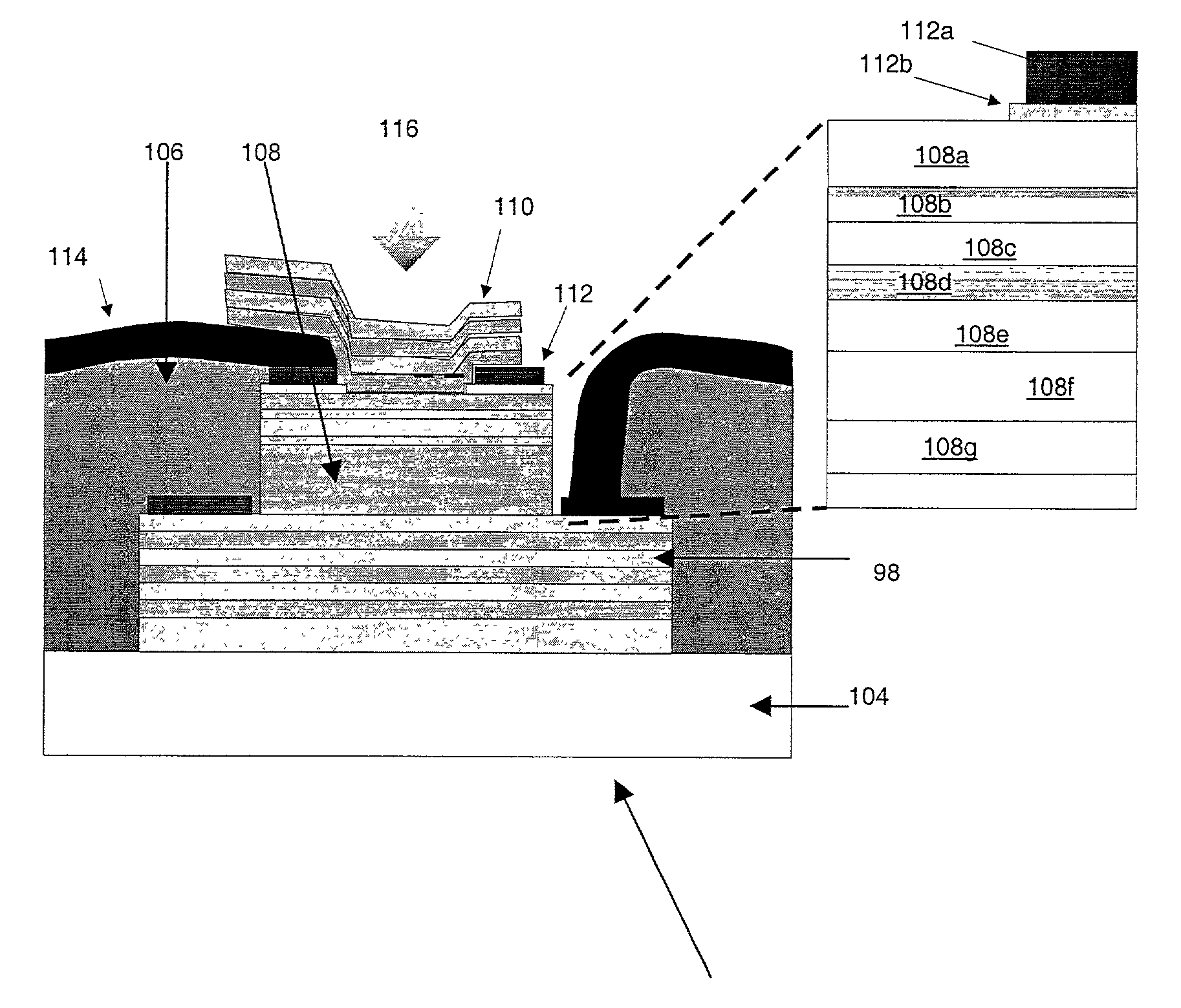
[0113]Operating wavelength may be one of the most significant specifications for a photodetector. For example, operating wavelength may determine an absorption material of a photodetector, and thus a material system for the whole device. In this manner, a semiconductor photodetector may be specified for an operating wavelength range. A long-wavelength cut-off of a spectral response may be determined by the absorption edge, or bandgap, of the absorption material of a photodetector. A short-wavelength cut-off may be observed because of recombination near the surface. Since optical fibers demonstrate minimum dispersion and attenuation at about 1.3 μm and about 1.55 μm, respectively, these wavelengths have become standards for long-haul high-bit-rate fiber optic telecommunication applications. For short-haul communications, such as local area networks (“LAN”), operating wavelengths may vary from about 800 nm to about 1 μm since the relatively inexpensive and well-developed AlxGa1−xAs an...


PUM


Abstract

An avalanche photodiode including a multiplication layer is provided. The multiplication layer may include a well region and a barrier region. The well region may include a material having a higher carrier ionization probability than a material used to form the barrier region.

Description

PRIORITY CLAIM[0001]This application claims priority to U.S. Provisional Application No. 60 / 236,952 entitled “Avalanche Photodiodes With An Impact-Ionization-Engineered Multiplication Region,” filed Sep. 29, 2000. The above-referenced provisional application is hereby incorporated by reference as if fully set forth herein.BACKGROUND OF THE INVENTION[0002]1. Field of the Invention[0003]This invention generally relates to avalanche photodiodes with an impact-ionization-engineered multiplication region. Certain embodiments relate to avalanche photodiodes having higher impact ionization in a first portion of the multiplication region and lower impact ionization in a second portion of the multiplication layer.[0004]2. Description of the Related Art[0005]Light has been used for communication since signal fires were first used to send messages thousands years ago. In the 1960's and 1970's, the invention of the laser and the development of the low-loss optical fiber have ushered in a new er...

Claims


Application Information

Patent Timeline
IPC IPC(8): H01L21/00H01L31/0328H01L31/107H01L31/109H01L31/18
CPCH01L31/107H01L31/1852H01L31/1075Y02E10/544
Inventor CAMPBELL, JOE C.YUAN, PING
Owner INTELLECTUAL VENTURES HLDG 40
Why Eureka
Try Eureka