Semiconductor device with metal gate and high-k tantalum oxide or tantalum oxynitride gate dielectric

a technology of metal gate and dielectric, which is applied in the direction of semiconductor devices, electrical equipment, basic electric elements, etc., can solve the problems of adversely affecting leakage current, leakage and thermal instability, micro-miniaturization engendering a dramatic increase in transistor engineering complexity, etc., and achieves the effect of reducing leakage current and reducing thermal instability

Active Publication Date: 2006-06-13
ADVANCED MICRO DEVICES INC
View PDF4 Cites 33 Cited by
  • Summary
  • Abstract
  • Description
  • Claims
  • Application Information

AI Technical Summary

Benefits of technology

[0006]An advantage of the present invention is a method of manufacturing a semiconductor device comprising a transistor with a replacement metal gate and high-k gate dielectric layer exhibiting reduced leakage current and reduced thermal instability.
[0007]Additional advantages and other features of the present invention will be set forth in the description which follows and, in part, will become apparent to those having ordinary skill in the art upon examination of the following or may be learned from the practice of the present invention. The advantages of the present invention may be realized and obtained as particularly pointed out in the appended claims.
[0008]According to the present invention, the foregoing and other advantages are achieved in part by a method of manufacturing a semiconductor device, the method comprising: forming a removable gate over a substrate with a gate dielectric layer therebetween; forming a dielectric layer over the substrate and exposing an upper surface of the removable gate; removing the removable gate leaving an opening in the dielectric layer; depositing a layer of tantalum (Ta) lining the opening; heating in an oxidizing atmosphere to convert the Ta layer into a high-k gate dielectric layer; and depositing a metal to fill the opening.
[0009]Embodiments of the present invention comprise depositing the Ta layer by physical vapor deposition (PVD) at a thickness of 25 Å to 60 Å. Embodiments of the present invention further include oxidizing the Ta layer in flowing oxygen or flowing ozone to form a high-k tantalum oxide gate dielectric layer, or in flowing oxygen or flowing ozone with flowing N2O to form a high-k tantalum oxynitride layer. Alternatively, oxidation can be effected in a plasma containing oxygen or ozone to form the high-k tantalum oxide gate dielectric layer, or in a plasma containing N2O and oxygen or ozone to form the high-k tantalum oxynitride layer. Annealing may optionally be conducted in an ammonia plasma subsequent to oxidation to form the high-k gate dielectric layer. A metal is then deposited filling the opening and planarization is implemented, as by chemical mechanical polishing (CMP), such that the upper surface of the metal filling the opening is substantially coplanar with an upper surface of the dielectric layer, thereby completing formation of the replacement metal gate electrode. Alternate embodiments include removing the gate dielectric layer before depositing the Ta layer.

Problems solved by technology

Micro-miniaturization has engendered a dramatic increase in transistor engineering complexity, such as the inclusion of graded well-doping, epitaxial wafers, halo implants, tip implants, lightly doped drain structures, multiple implants for source / drain regions, silicidation of gates and source / drains, and multiple sidewall spacers.
Typically, the structural and doping parameters tending to provide a desired increase in drive current adversely impact leakage current.
Carbon is believed to be a major source for leakage and thermal instability.
Replacement of conventional CVD or ALD deposition tools is very costly.

Method used


Image

  • Semiconductor device with metal gate and high-k tantalum oxide or tantalum oxynitride gate dielectric
  • Semiconductor device with metal gate and high-k tantalum oxide or tantalum oxynitride gate dielectric
  • Semiconductor device with metal gate and high-k tantalum oxide or tantalum oxynitride gate dielectric

Examples


Embodiment Construction

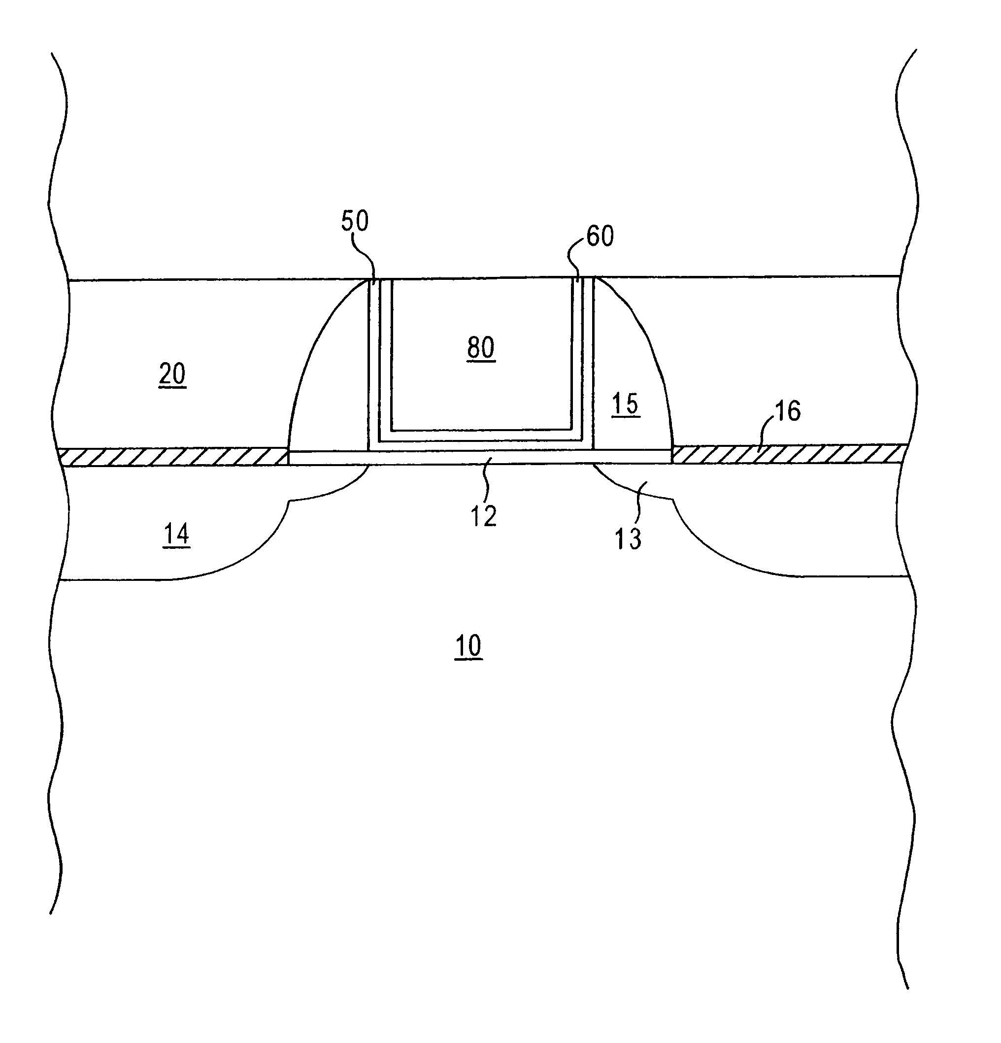
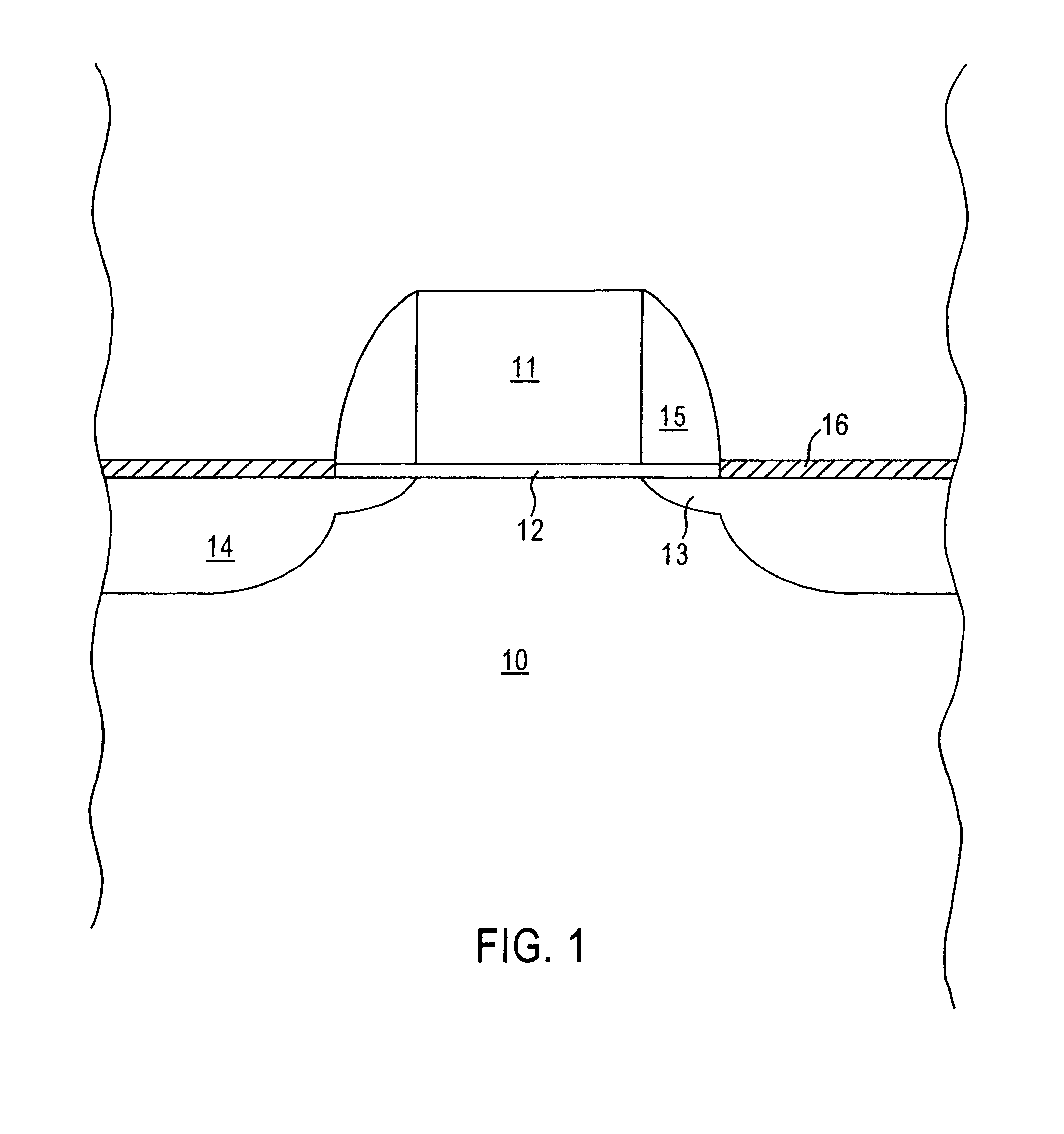
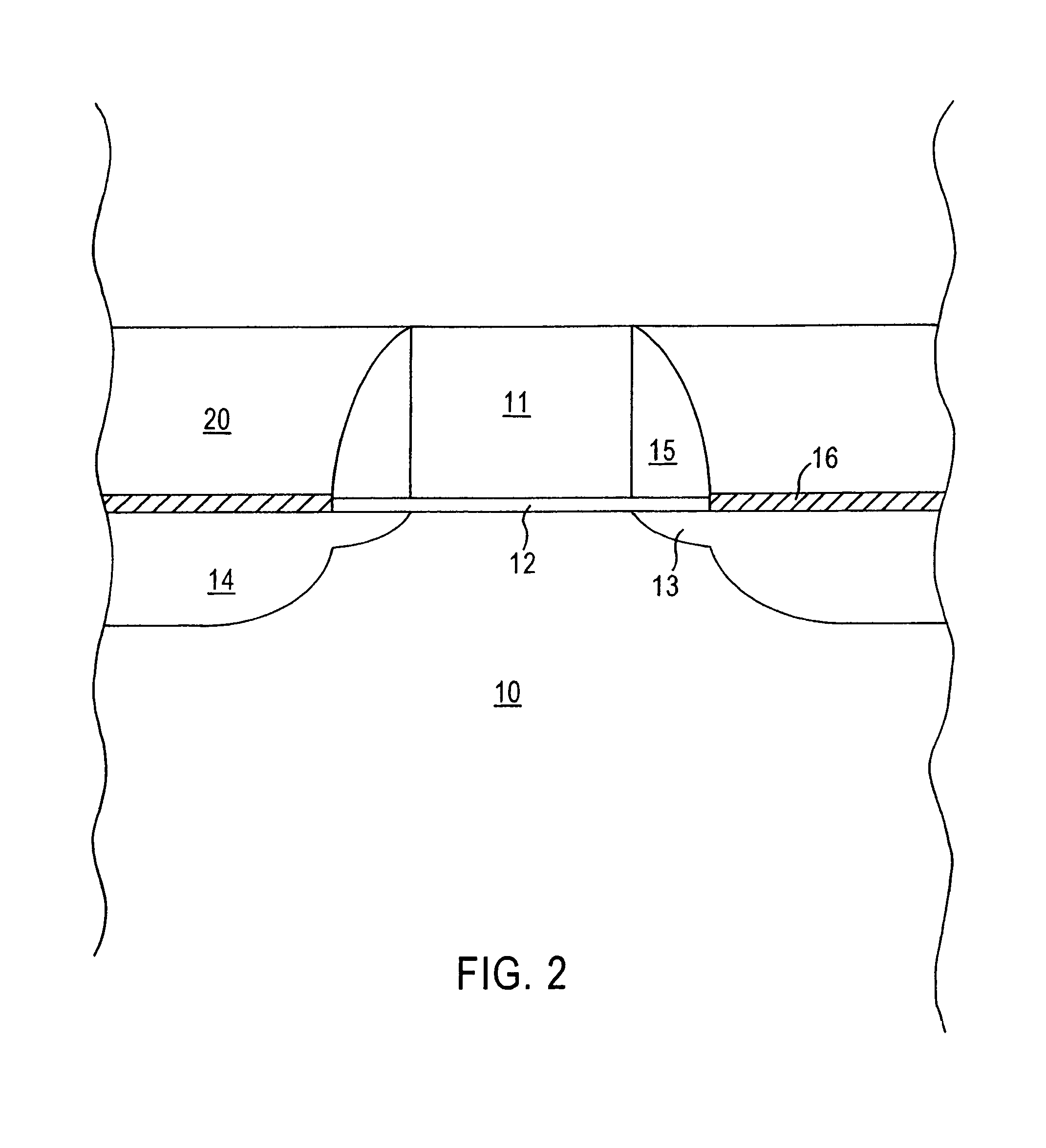
[0014]The present invention address and solves problems attendant upon conventional semiconductor devices comprising polysilicon gate electrodes having high resistivity and, hence, slow operating speed. The present invention also addresses and solves problems attendant upon conventional replacement metal gate methodology and conventional techniques employed to form high-k gate dielectric layers for use with replacement metal gates. The present invention addresses and solves such problems by providing methodology enabling the fabrication of transistors with a replacement metal gate electrode and a high-k gate dielectric layer, such as a high-k tantalum oxide or tantalum oxynitride gate dielectric layer, having significantly reduced carbon and, hence, significantly reduced leakage and significantly reduced thermal instability.

[0015]In accordance with embodiments of the present invention, a removable gate electrode is removed and a thin layer of Ta is deposited by a conventional PVD te...


PUM

PropertyMeasurementUnit
temperatureaaaaaaaaaa
temperaturesaaaaaaaaaa
dielectric constantaaaaaaaaaa

Abstract

Microminiaturized semiconductor devices are fabricated with a replacement metal gate and a high-k tantalum oxide or tantalum oxynitride gate dielectric with significantly reduced carbon. Embodiments include forming an opening in a dielectric layer by removing a removable gate, depositing a thin tantalum film, as by PVD at a thickness of 25 Å to 60 Å lining the opening, and then conducting thermal oxidation, as at a temperature of 100° C. to 500° C., in flowing oxygen or ozone to form a high-k tantalum oxide gate dielectric layer, or in oxygen and N2O or ozone and N2O ammonia to form a high-k tantalum oxynitride gate dielectric. Alternatively, oxidation can be conducted in an oxygen or ozone plasma to form the high-k tantalum oxide layer, or in a plasma containing N2O and oxygen or ozone to form the high-k tantalum oxynitride gate dielectric layer.

Description

FIELD OF THE INVENTION[0001]The present invention relates to the fabrication of semiconductor devices comprising transistors with metal gate electrodes and high dielectric constant (k) gate dielectric layers exhibiting reduced leakage and improved thermal stability. The present invention is particularly applicable to fabricaturing high speed semiconductor devices having submicron design features.BACKGROUND ART[0002]The integration of hundreds of millions of circuit elements, such as transistors, on a single integrated circuit necessitates further dramatic scaling down or micro-miniaturization of the physical dimensions of circuit elements, including interconnection structures. Micro-miniaturization has engendered a dramatic increase in transistor engineering complexity, such as the inclusion of graded well-doping, epitaxial wafers, halo implants, tip implants, lightly doped drain structures, multiple implants for source / drain regions, silicidation of gates and source / drains, and mul...

Claims


Application Information

Patent Timeline
Patent Type & Authority Patents(United States)
IPC IPC(8): H01L21/336
CPCH01L21/28079H01L21/28229H01L29/66545H01L29/4958H01L21/28088H01L29/4966H01L29/517
Inventor NGO, MINH VANWOO, CHRISTYPAN, JAMESBESSER, PAUL R.YIN, JINSONG
Owner ADVANCED MICRO DEVICES INC
Why Eureka
Try Eureka